Nanopocket Membrane Fabrication-Update
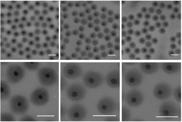
This is a continuation of the silicon substrate bias series. I have added several more data points to highlight the trend. Below are the TEM micrographs, pore distributions, average diameter/porosity/density plots. It would appear that the “optimal” bias is at 05W if we are using porosity as a metric. I also performed a short temperature…
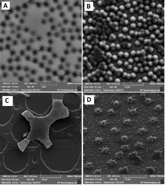
After the w310 series being beautiful (few pinholes, reasonable strength, high yield), we have retreated somewhat with a return of the copper-related piholes. Here is an SEM image and EDX scan from the well wall: Here is a pic of a pinhole on the membrane with a telltale copper silicide particle attached to the edge:…
We are proposing a novel method for the fabrication of porous thin-film silicon membranes. It has been shown that metallic nanoparticles on the surface of silicon submerged in a solution of hydrofluoric acid and hydrogen peroxide will bore holes into the silicon. This selective etching occurs because the metal acts as a catalyst in the…
First off – OK now on to the science. Wafer 747 has a huge amount of pinholes, and in this study I wanted to see how these pinholes would effect electroosmosis. I will show results here from two experiments with these holey membranes. These membranes have a lower rate of electroosmosis than previous tested membranes. …
Along with differently sized square membranes, I also designed a wafer with different sizes of slits. On each chip, there is a 4000, 2000, 1000 and 500um long window. The thicknesses of these windows are 200, 100, 50 and 25um. I’m interested to see if there is an aspect ratio that causes endothelial cell alignment/tubulogenesis. …
I’ve always suspected that the pore formation process was very quick and to confirm this I looked at a wafer that was annealed for 10 s vs. 60 s. From the distributions, it would appear that the majority of pores nucleate and grow during the ramp and first few seconds of steady state. Next, I…