Update on NPN Liftoff
This is a summary I wrote ~3 weeks ago of the work Josh Miller and I are doing under the CEIS grant for NPN Lift-off.
Summary: Josh and I have been working for about four weeks so far on this program. During that time we have done preliminary lift-off (LO) tests on two wafers: one with micropores (~600 µm thick wafer) and one with the nanoporous transfer (300 µm thick wafer). We are able to get LO with the microporous SiN film (50 nm thick, 3 µm diameter pores, 6 µm center-to-center pitch). It was found that a thin layer of silicon dioxide on top of the nitride is needed to achieve sufficient adhesion of the SU-8 microgrid scaffold. Tests with the nanoporous membrane showed mixed LO results. We feel a major source of the issues is that the sacrificial poly-Si film that was put down under the 50 nm SiN film is very bumpy with features on the order of ~100 nm. Additionally, there were some issues with the deposition of the silicon dioxide adhesion layer, which has resulted in poor adhesion of the SU-8 layer. The results are summarized below and our list of next steps are provided at the end.
Microporous:
Bob patterned one of the old wafers that Josh had gotten coated with SiN after depositing the thermal oxide/poly-Si stack. These were intended for use in developing nanoporous nitride, but it was found that pnc-Si could not be formed in the RTP step since these are thicker wafers than the usual, double-side polished ones. High porosity, ø3 µm pores were patterned using RIE. I attempted to apply SU-8 to the nitride surface but found that the SU-8 did not adhere well. I added ~30 nm of TEOS SiO2 per Josh’s recommendation. The SU-8 stick very well to this. I broke out a couple 1 in2 pieces to test LO with. These were dipped in 10:1 BOE w/ surfactant for ~60 s to remove the TEOS and native oxide in the pores. I found that I could get membrane lift-off with seven pulses of XeF2 in the Xactix, which is perhaps a little bit slow compared to Josh’s previous experience. This could likely be explained by a slightly incomplete oxide strip. Still, the tests are encouraging in that the basic process for microporous nitride LO seems to be working.

Figure 1: SEM micrographs of microporous nitride taken at RIT’s Nanoimaging Center.
NPN:
Back in August, Josh provided me with three double-side polished wafers with 100 nm thermal oxide to be coated with poly-Si during a run I was doing for the SiO2 oxide project. I deposited ~750 nm of poly-Si. The wafers were then run through RCA cleaning and sent to Rouge Valley for deposition of 50 nm of SiN. Josh deposited a-Si + oxide on one of these, ran it through RTP, and then ran it through nanoporous transfer at RIT in the RIE process. Prior to applying SU-8, Josh attempted to apply ~30 nm of TEOS, but there seemed to be issues with the P5000 tool, and it seemed that no oxide was actually deposited. He tried again the next day when JP was running the tool for some other SiMPore wafers. We tried to measure the SiO2 thickness using the Nanospec Spectrophotometer out in the edge region of the wafer, but we weren’t able to get conclusive numbers. Bob applied and patterned the SU-8, and it seemed to be adhering well through the development process. However, once the wafer was cleaved and we dipped a couple in 10:1 BOE solution to strip the oxide, we found that the SU-8 grid was separating from the wafer pieces. Josh is fairly confident that this issue was caused by a temporary malfunction with the TEOS deposition tool, since he has had obtained good adhesion of SU-8 to nanoporous nitride before using this method.
We attempted to do LO using XeF2 with these pieces and found that while some through-pore etching occurs, it was not uniform across the sample, and seemed to be very slow compared with the microporous LO. In Figure 2, one can see that some of the open squares are etching faster than others. When the samples were dipped in the BOE solution, we noticed that some of the regions did not wet easily because of the hydrophobicity of the SU-8. Likely the squares that show little through-pore etching are ones that did not get wetted by BOE during the oxide strip. Note that even though we think little on no SiO2 was deposited by TEOS deposition, there will still be a native oxide on the surface of the poly-Si that needs to be stripped to get efficient through-pore etching with XeF2.
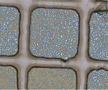 Figure 2: Optical micrograph of NPN sample after three pulse of XeF2. The blue spots represent areas where through-pore etching has occurred Note that the regions in the lower left appear to have less etching; this is thought to be a result of incomplete native oxide stripping.
We then tried using the vapor HF stripping fixture to remove the native oxide. Bob first tried placing a 1 in2 sample in the fixture face up for 20 minutes. After exposing the sample to three pulses of XeF2, it was apparent that the sample was showing signs of lifting off around the edges. As with the earlier samples that were dipped in BOE, the SU-8 was found to delaminate during the DI water rinse after treatment in the vapor HF fixture. Also, as seen in Figure 3, it is apparent that the sample did not get an even exposure to HF vapor across its face, and that we should probably place the samples face-down to improve this.
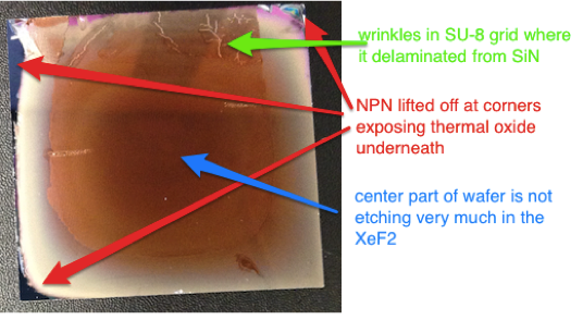
Figure 3: Photograph of NPN LO sample (~ 1 in2) after three XeF2 pulses that had undergone a 30 min. vapor HF strip. Note that the center region of the sample does not appear to be etching effectively, which indicates that the native oxide was not removed there by the vapor HF treatment. NPN membrane lift-off at the corners (shown in better detail in next figure).
Figure 4 shows more detail of the corner of this sample illustrating that on the order of a couple mm2 of the NPN membrane has separated from the substrate. This is encouraging since the degree of LO seen indicates effective, through-nanopore etching of the XeF2. The length scale of etching (mm) is too long to have all occurred from the edge. Following this, Josh treated some samples in the vapor HF fixture face down for 15 minutes. When put in the Xactix, but the degree of through pore etching after three pulses was very low, so we put the samples back in the vapor HF fixture for an additional 15 min. Following this, the sample did seem to be progressing fairly well in successive pulses. It was exposed to a total of 9 additional pulses beyond the 1st three it got before the second vapor HF treatment. Following this, Josh used tweezers to liftoff the sample and transfer it to a gelbox that had some empty TEM grids. We noticed that the NPN membrane only transferred with the SU-8 grid around the outer part of the sample. When we looked at the sample under the light microscope afterward, it was clear that the through-pore etch was incomplete under the SU-8 intersections in the middle ~ 1/3rd of the sample (sorry no photographs or micrographs, yet). Josh took the sample to UR to do imaging. First, he was not able to do STEM analysis on the membrane samples that were suspended over open TEM window because they would disintegrate under the beam energy when he attempted to focus on a region. Further, the surface of the sample on the chip shows that the poly-Si surface is very bumpy (see Figure 5). It’s not clear whether this was the state of the poly-Si upon deposition in LP-CVD or from undergoing RTP when forming the pnc-Si. In either case, it is almost certainly messing up formation of good nanopores in the a-Si during RTP and the subsequent transfer to SiN. Also, if it was present to begin with, it probably reduces the strength of the SiN film.
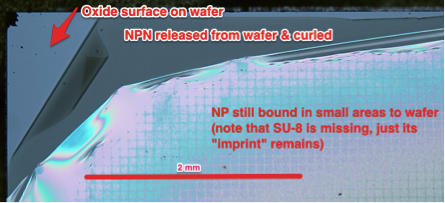

Figure 4: Micrographs of NPN-LO sample that was exposed to 30 min. of vapor HF strip and 3 pulses of XeF2. The SU-8 grid delaminated during the DI water rinse following vapor HF treatment, but there is encouraging evidence of NPN-LO
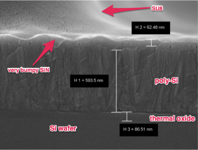 Figure 5: SEM micrograph of cross section taken from NPN-LO sample region where the membrane did not lift off. The surface of the poly-Si is very bumpy, which is likely interfering with the integrity of the SiN layer, the formation of the nanopores in pnc-Si during RTP, and the transfer of the nanopores during the transfer RIE
Josh got a sample wafer from Rogue Valley that was coated with their version of LP-CVD Poly-Si and examined this against one of our LP-CVD poly-Si in the UR AFM instrument. Below are images of the two:
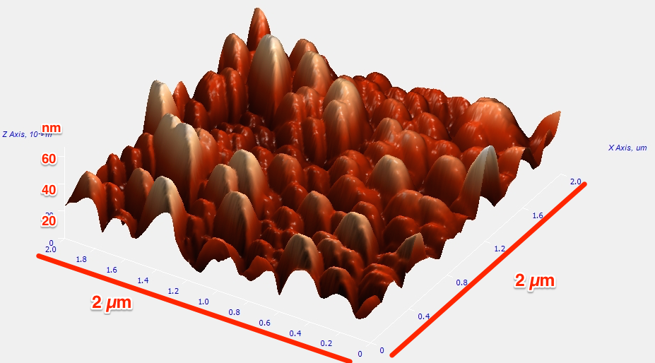
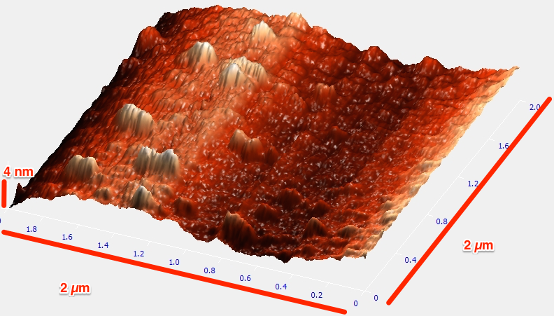 Figure 6: AFM images of RIT (LEFT) and Rogue Valley (RIGHT) Ploy-Si layers showing the significant difference in surface roughness.
Below are the summaries of the surface roughness measurements:
both are 2 µm x 2 µm
RIT: