Wafer 612 and 615
Wafer 612 was made to mimic wafer 504: 850 C RTP, cool down, 1000 C RTP. Wafer 615 was annealed in two steps: first to 400 C and then to 1000 C (without inbetween cool down). Both wafers showed a lower pinhole density. Wafer 615 had a few “traditional” round pinholes. Wafer 612 had some membranes with tears, especially along the edges.
Karl mentioned in his post that he saw dark features concentrated inside water spots. Under the TEM, it was verified that these dark features are not pinholes but just organic contamination. The spots are probably coming from a dirty Pentane solution (since been changed out).
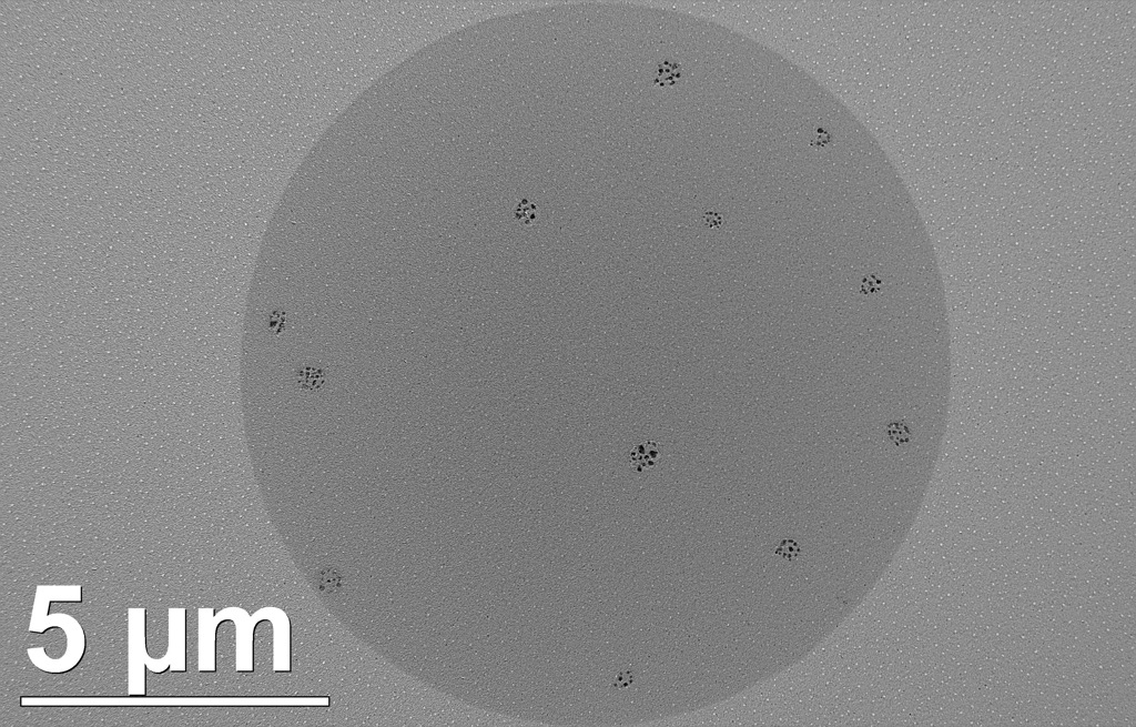
Wafer 612
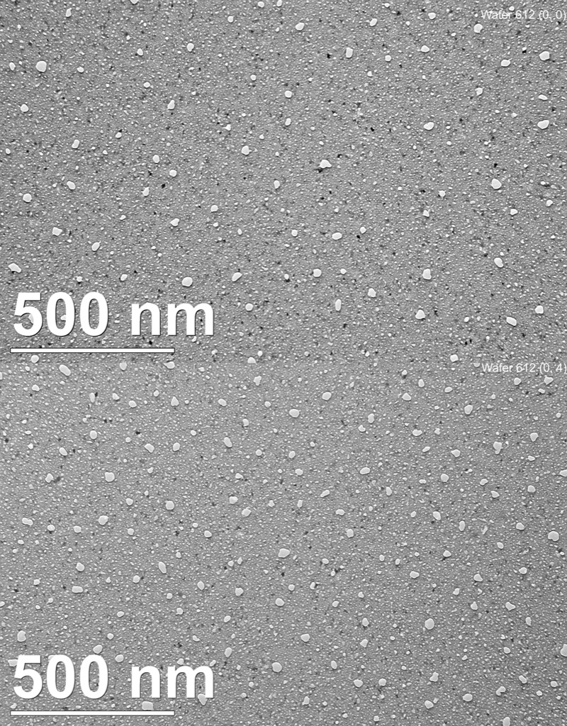
Wafer 615
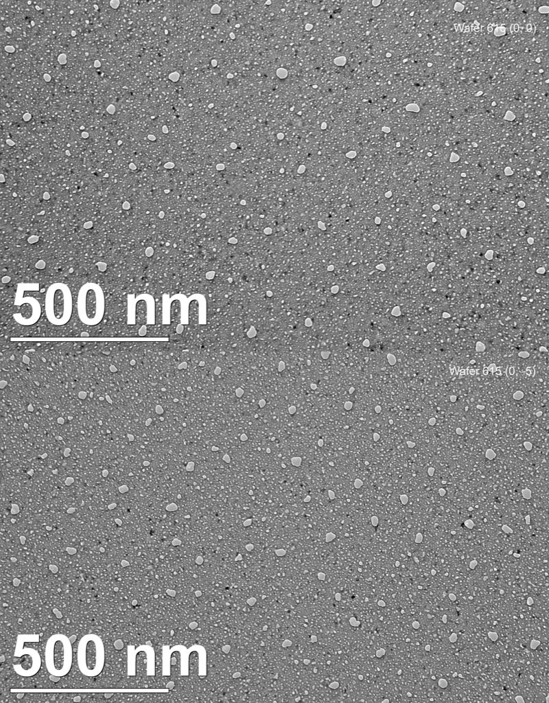
Both 612 and 615 have cutoffs around 40 nm.