Central Composite Design for Optimizing SERS Substrates
Now that we have a number of ways to quantify the nanostructure of different npMgF2/npAu film stacks, we can begin an optimization experiment for which combination of factors will be useful to us. To explore the space of outcomes, we have a set of Factors at a certain number of Levels. These produce a set of Responses that we can quantify. For complicated processes, there may be many factors at work and the experiment space can be rather large. Factors can be thought of as physical dimensions or process settings. Some potential factors in my npMgF2/npAu fabrication.
Factors (Process Settings)
- Au thickness
- MgF2 thickness
- Au-MgF2 thickness difference
- NPN Pore Distribution
- NPN Pore Range
- Etch Type
- Etched NPN
- Deposition Temperature
- Deposition Rate
Factors (Physical Dimensions)
- MgF2 Pore Distribution
- MgF2 Surface Roughness
- Au Thickness
Responses
- SERS thiophenol SNR
- SERS thiophenol background variation
Through my course of manufacture over the last months, I have begun exploring some different factors to see if there are reasonable explanations for their effect.
Factors (Process Settings)
- Au thickness
- Changes the plasmon generation condition.
- MgF2 thickness
- Changes the nanopore infill, surface roughness
Au-MgF2 thickness difference- Fixed as a combination of Au/MgF2 thicknesses.
NPN Pore Distribution- Fixed for this experiment. Wafer 1236 has a certain distribution
NPN Pore Range- Fixed for this experiment. Wafer 1236 has a certain distribution
Etch Type- Many different types of etch do not appear to change morphology of NPN, under TEM.
Etched NPN- Residual NPN will effect plasmon generation. Process fixed as removing NPN.
- Deposition Temperature
- 150C, 250C, 350C have different grain structures
Deposition Rate- Fixed at 0-2 A/sec. Faster depositions lead to more irregular surfaces.
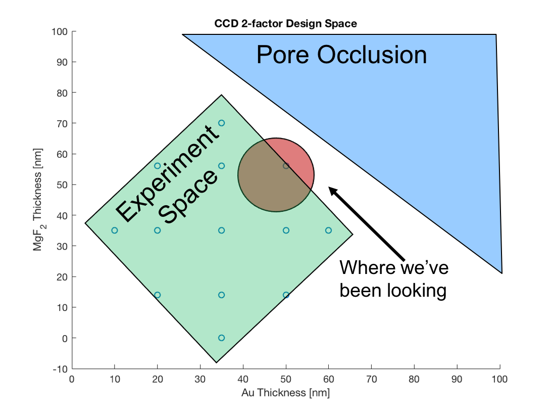
We now have a reasonable number of factors to investigate. The next step is to pick levels that will produce significant differences from treatment to treatment. There is some prior knowledge involved here. We have an idea of what an appropriate range of Au or MgF2 thicknesses, deposition temperatures might be. Knowing this, we can draw out an experimental space.
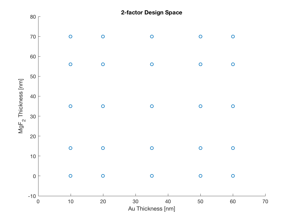
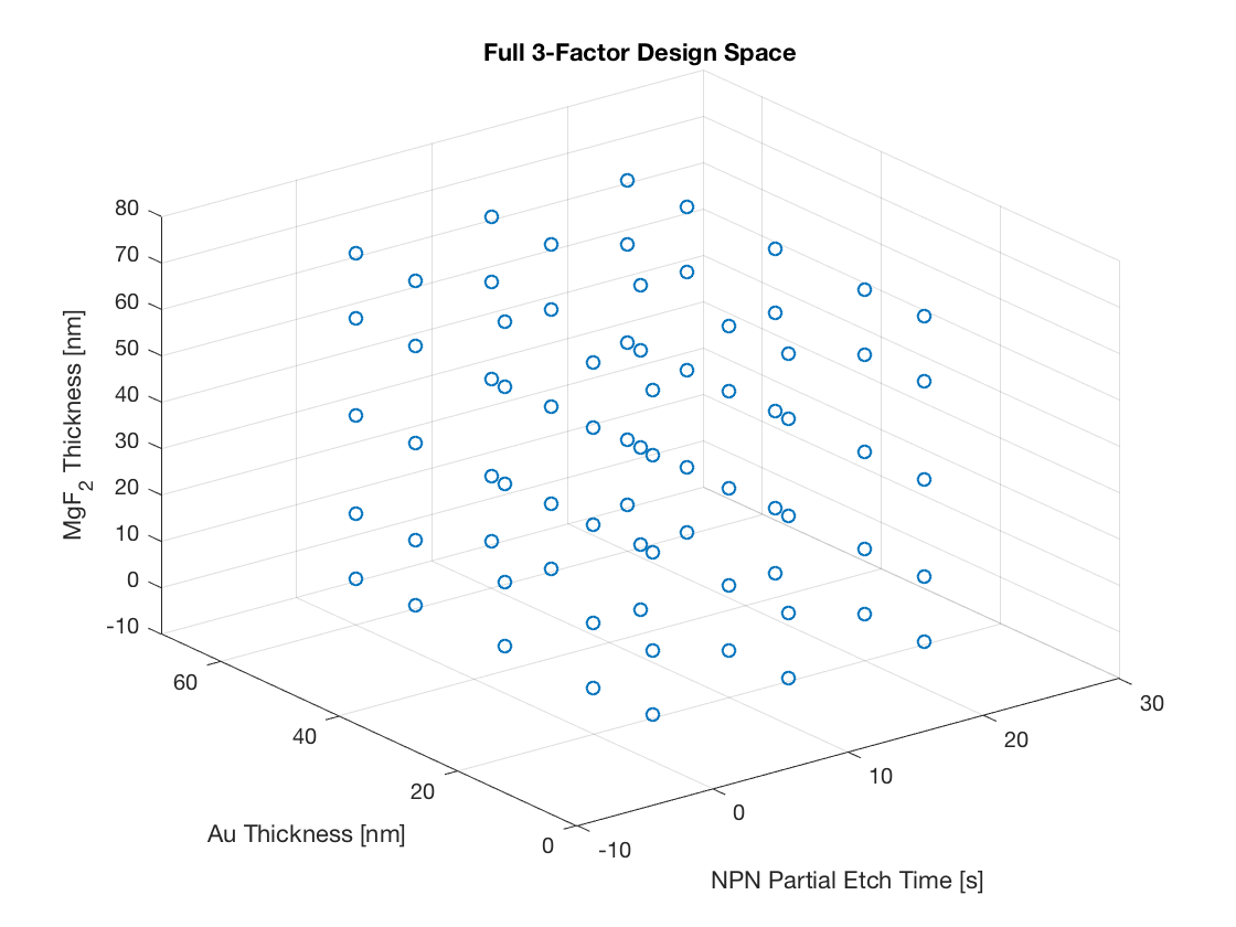
These experiments are complete, but they require a lot of material and a lot of different process conditions. A Central Composite Design helps to maximize the efficiency of this area. Since we want to explore significant differences at our chosen levels, we can modify the experimental space to look more efficiently. Most responses do not have multiple significant optimums. If we center on the point we believe will give us the best response, we can search the outer edges more efficiently.
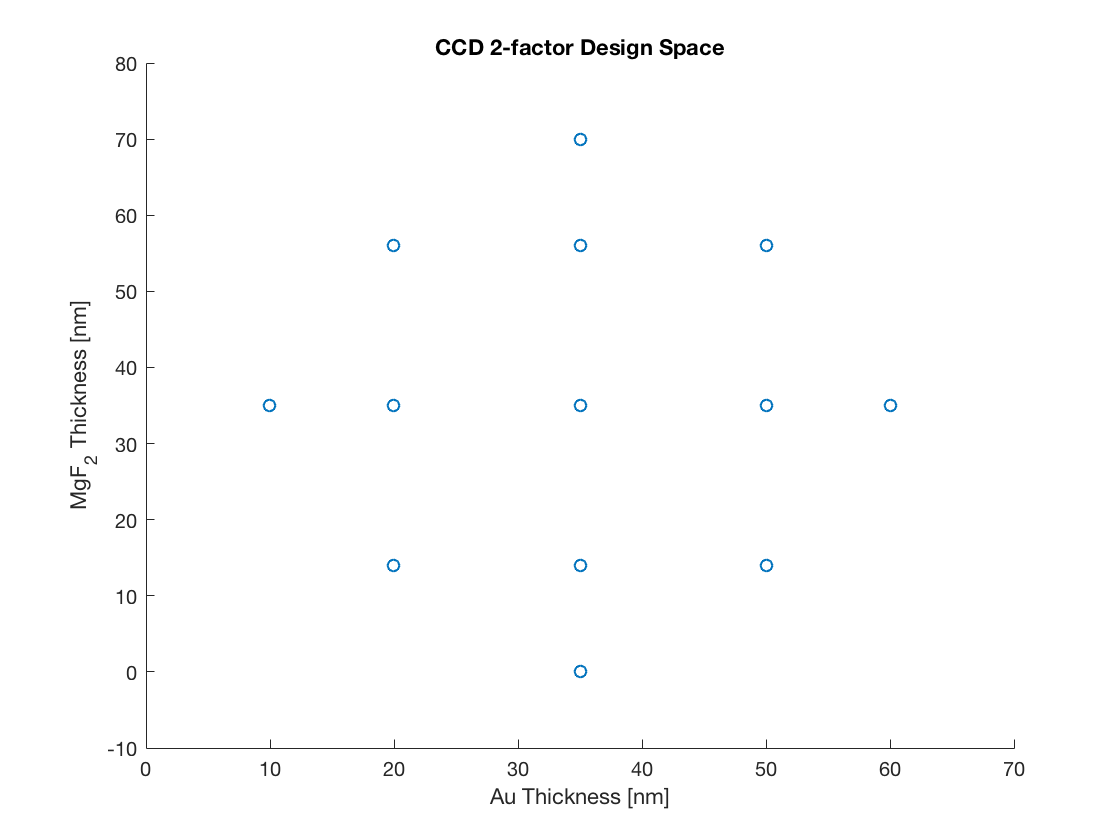
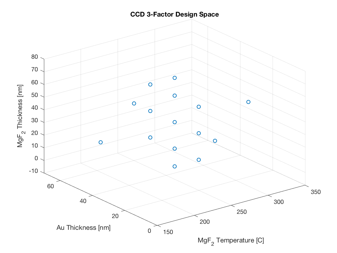
Designs like these allow us to use a number of chips well to get the required information. Mathematically, we can run ANOVA to examine if the factors contribute significantly to the response, and then create an surface for optimization.