SiN-NP in 50 nm SiN
Using a 6″ wafer, we start with 50 nm of RV SiN, then deposit 40 nm a-Si followed by 20 nm of SiO2. RTP of 1050 C, 100 C/s, 60s. JP patterned the wafer to make standard SEPCON chips.
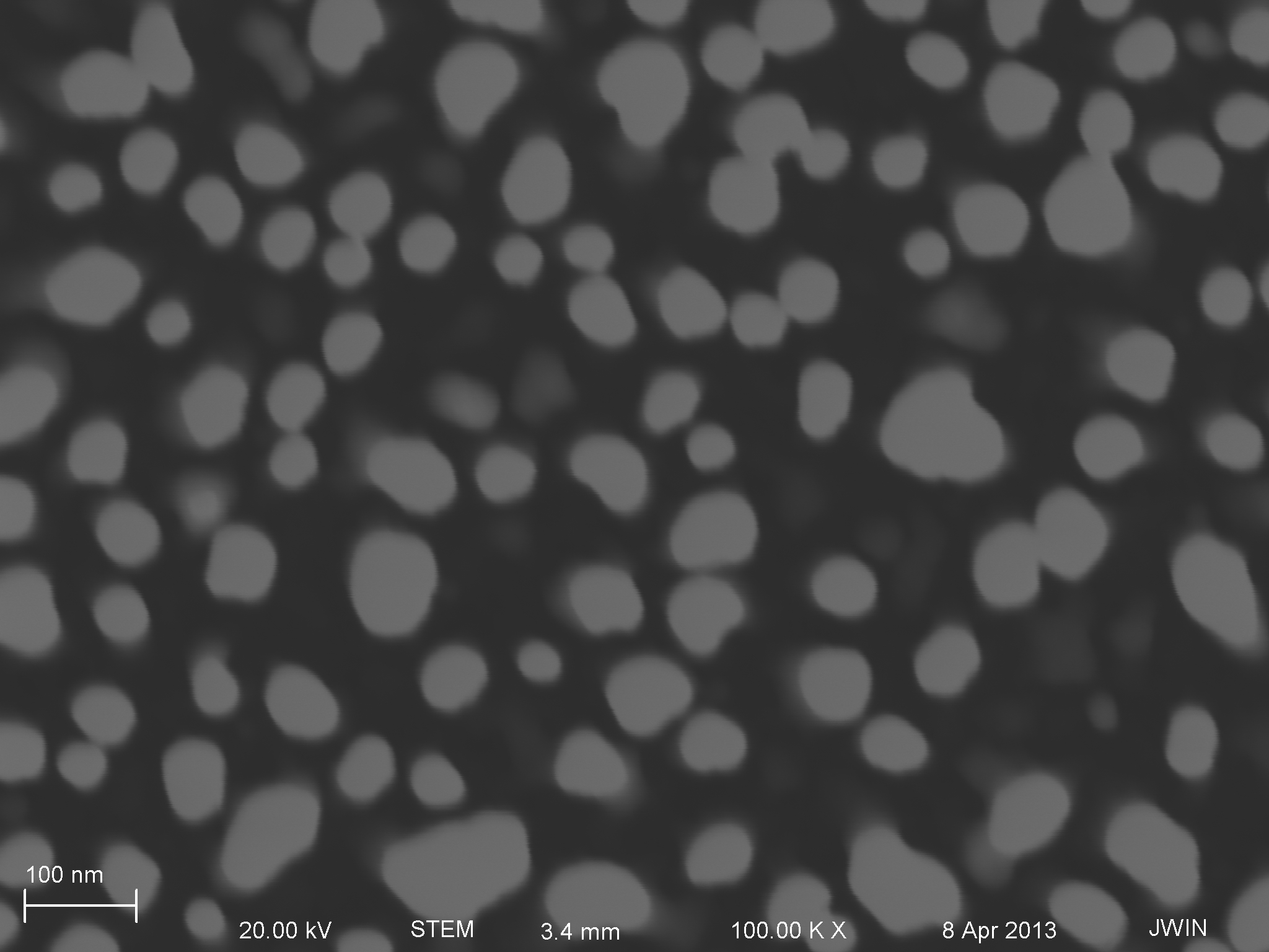
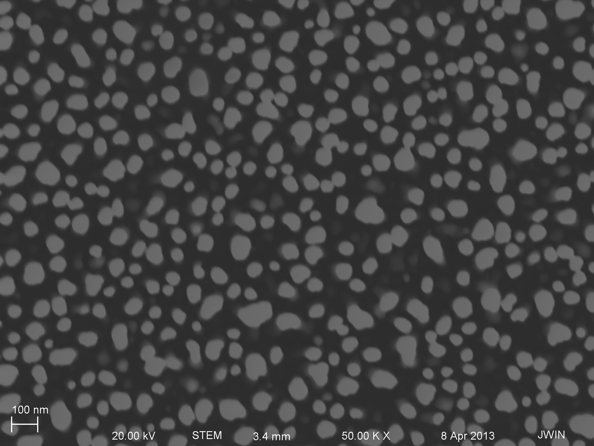
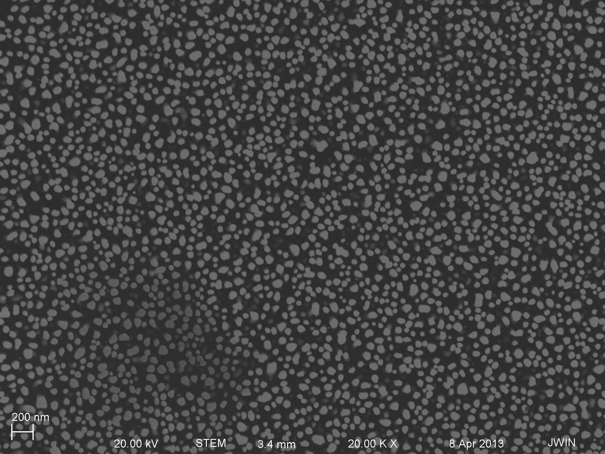
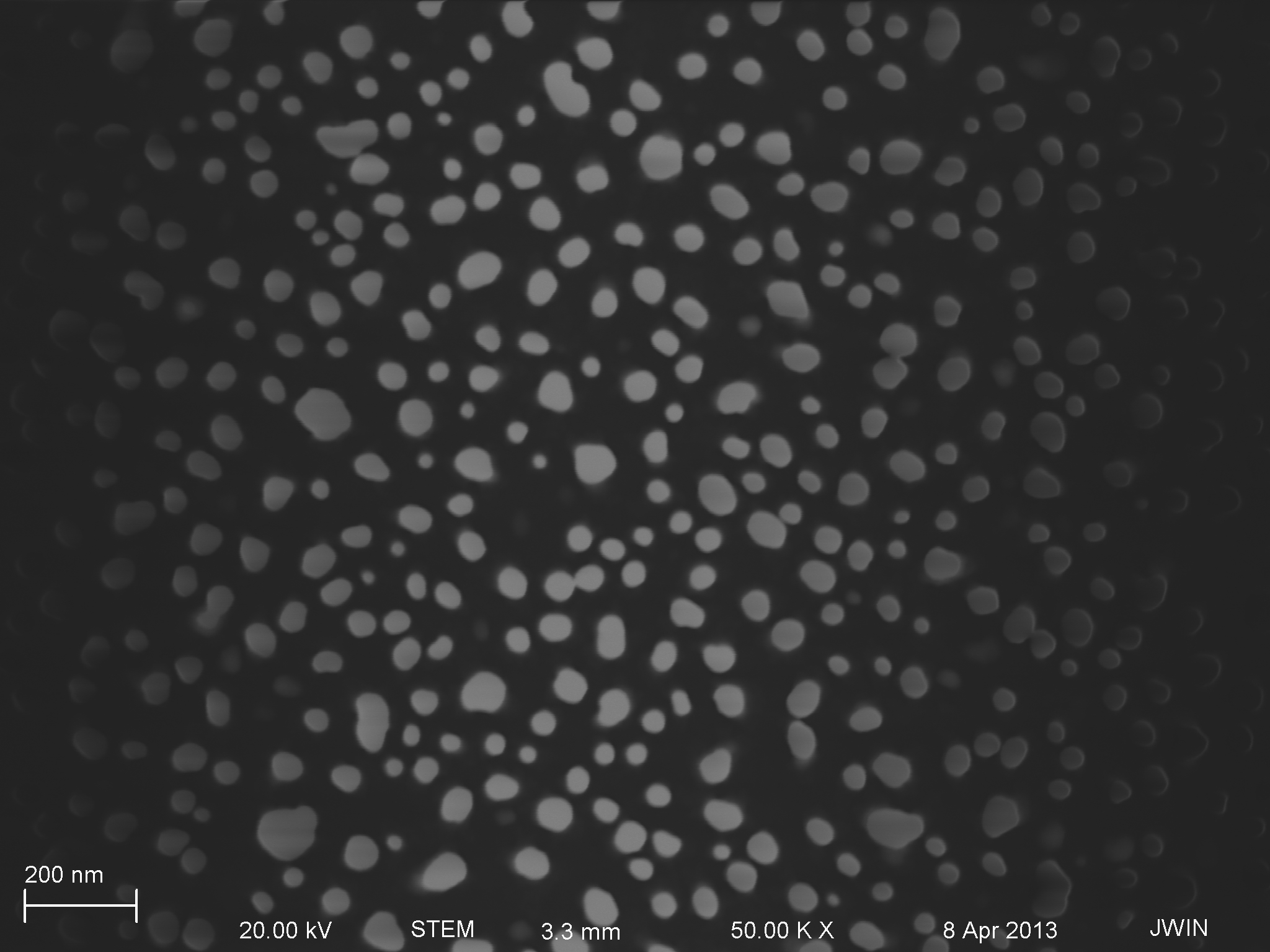
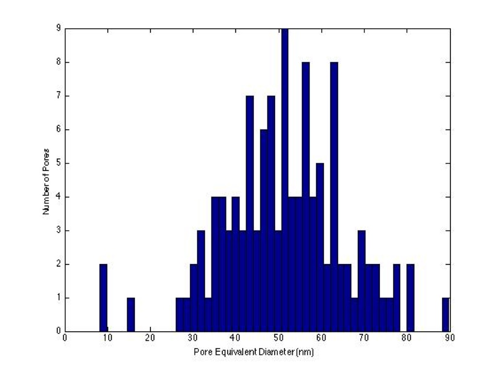
The pores were transferred to the SiN using RIE. The RIE etches faster at the perimeter of the wafer than in the center. The porosity/avg. pore size at the perimeter is 30%/61 nm and at the center is 27%/54 nm.
The max burst pressure at the perimeter was 17 psi and in the center a sample withstood up to 32 psi. (the current setup maxes out 32 psi so we can’t test higher pressures)
Karl tested the the hydraulic permeability of a few samples using 4.7 psi on the constant pressure test setup.
perimeter ~9800 µL/min/psi/cm2
center ~5400 µL/min/psi/cm2
(We used the matlab code from the NRG blog to calculate a theoretical hydraulic permeability:
perimeter ~20,000 µL/min/psi/cm2
center ~14,400 µL/min/psi/cm2)
The following 3 STEM images are from a sample near the perimeter of the wafer.

Here is a sample with slightly lower porosity/pore size from the center of the wafer.
This is unequivocally good news.