Bonding silicone gaskets with nanoporous nitride (Solved ?!?)
In order to resolve the silicon nitride- silicone gasket bonding issue, I, Josh, Tucker and Greg used different approaches to functionalize the nanoporous nitride (NPN) surface. Both surfaces of NPN, although have same material (silicon nitride), behave differently. The flat side is etched using xenon fluoride to remove pncSi layer on top.
Different tools at our disposal:
1) YES system (UR Nano)
2) UV-Ozone (UR equipment room)
3) Tube furnace (UR Nano)
4) RTP (UR Nano)
5) Oxygen Plasma (Brian’s lab)
6) RIE (UR Nano)
Results obtained after using different tools:
1) RIE: We found this small tutorial from someone from Whitesides’ group. Using their parameters (1 sccm oxygen, 200 mTorr, 125 W for 1 min), we (Greg and I) exposed the chips and the gaskets inside the RIE hoping that it will oxidize the chips. It didn’t work, and neither pncSi nor NPN surfaces sticked to the gasket. We didn’t bother to give it another shot.
2) Oxygen Plasma: We (Josh and I) used the Oxygen Plasma (Southern Bay Technology) to oxidize the NPN surface. Using 100 W Forward Power (with ~4 W reflected power), 200 mtorr pressure maintained by adjusted O2 flow rate, we exposed the surfaces for about 15 mins. Yet again, NPN surfaces didn’t stick to the gaskets. No second attempt at this tool either.
3) UV Ozone: Multiple attempts were performed to use the conventional UV Ozone treatment for this bonding. Neither of Tucker, Dean or I got any success in doing this. Being the weakest of all the tools, this doesn’t seem surprising now!
4) Tube Furnace: Josh put some chips inside this furnace at 1100C for 1 hour. Josh didn’t check for gasket bonding because the windows were wrinkled. (One chip was analyzed in XPS, results pending)
5) YES system: Tucker played with multiple parameters to use YES system for bonding. He tried different orientations (flat side up or trench side up), time (840 s or 1800 s) and placement inside the YES system (top shelf or bottom shelf). Summarily, he was able to get weak bonding on the flat side, but no bonding of whatsoever strength on the back side in either of the conditions.
6) RTP: After all these tests, it was realized that functionalization of native nitride surface is not going to help us in bonding it to the gaskets. Josh found an old paper, which mentioned that higher temperature treatment in oxygen rich environment is the key to create an oxide layer on the surface, which then can be optimized for silicone bonding. Paper can be found here.
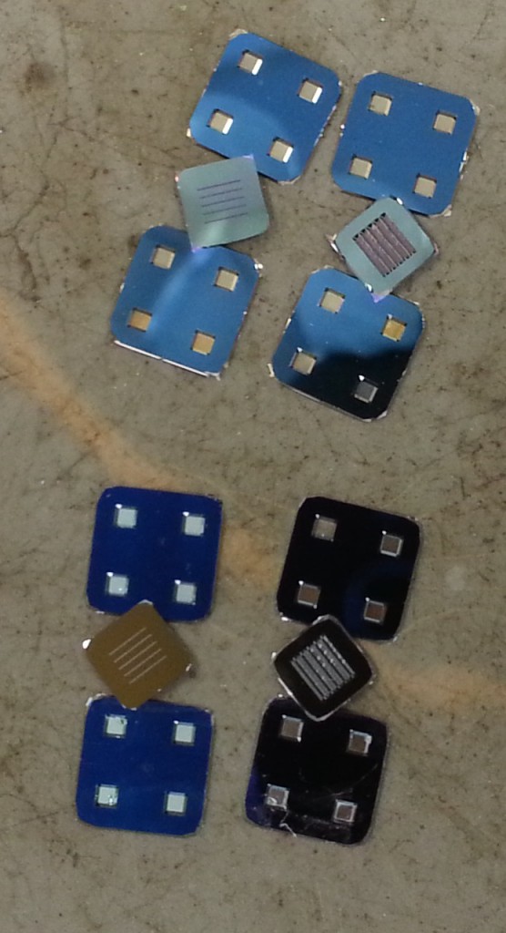
So Josh and I ran the RTP at several different temperature cycles starting from 1100 to 700 C for different time intervals. Main observation was: the NPN wrinkles at T>900 C. Second observation: 1 min exposure to 900 C was sufficient in making the bonding (both the sides) happen, but it takes longer time (5 min) if we are doing at lower temperatures. As of now, I am doing RTP at 700 C for 5 mins in 1 sccm flow of oxygen and 5 sccm argon, with the bottom section of the susceptor (no lid). I created a new recipe on the tools for that, which spikes up to 730 C and stabilizes eventually at 700 C within 90 sec. Using this recipe, I tested NPN chips from wafer 1070. I placed two CytoVu chips acting as a spacer, and suspended NPN chips on the top of that, one facing up and one facing down, as shown in the picture below.
We alternated the orientation of the samples to control for different exposure to the lamps and gas flows. After RTP I immediately treated the chips using UV Ozone system. The gaskets and samples exposed for 15 mins at ~ 1 L/min oxygen supply. Instead of baking them in oven after this, I flipped the chip-gasket assembly, and treated the second surface as well in UV Ozone using same parameters for gasket bonding. After both the sides were sandwiched by gaskets, I put them in oven at 75 C for 1 hour. Both the sides were irreversibly bonded to the gaskets. Upon inspection, I noticed that some of the windows were broken, but that’s entirely due to my expertise in handling the chips. No wrinkles were observed. The treatment worked 🙂
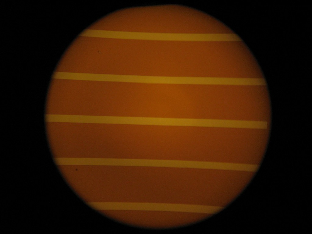
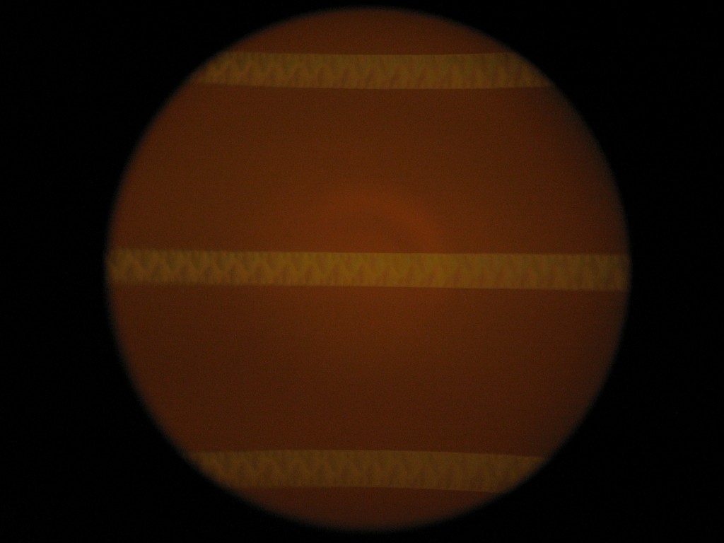
Some images of wrinkled and unwrinkled membranes:
RTP at 700 C for 5 mins

RTP at 900 C for 1 min
RTP at 1000 C for 1 min (wrinkles)

I also worked with microporous silicon nitride membranes (#4369) and put them through same processes. The results with that material were quite different. The windows never showed any wrinkling or other damage, even at 1100C. The bonding results were quite inconsistent, some temperature runs showed bonding to flat side, but not the trench side, while some other runs showed vice versa. More exhaustive and conclusive studies need to be made in the case of microporous material.
Even for the NPN, there are many other parameters that need to be explored:
1) Is 700 C actually required, or can get away at lower temperatures?
2) Is 5 mins required or lesser time durations can work? 1 min at 700 C didn’t work.
3) Oxygen flowrates?
4) Positioning of the chips in the susceptor … Will it make a difference if the whole wafer is RTPed or individual chips need to be handled?
5) How long after the RTP, or how soon, does the UV oxidation need to be done? Can we use YES system now?
6) Finally, how does it affect burst pressure, pore radius and other properties?
This work was only a proof-of-concept to lay out the foundation for a more detailed study.
That’s all folks!
To give a more complete summary of my experiment and what I’ll be doing about this in the future, I’ll post it here:
A test was performed on 16 SiN CytoVu chips, regarding their ability to form irreversible bonds with PDMS after plasma treatment in the YES system with three varying parameters: top vs. bottom shelf, 840s vs. 1800s plasma treatment, and upright vs. inverted. Two chips were tested in each combination of the parameters and then left to form bonds with PDMS gaskets for ~20 hours at 60 degrees celsius.
None of the chips formed strong bonds with the PDMS. The chips which were inverted invariably failed to form any bond whatsoever, while the upright chips formed very weak to moderately weak bonds (none passable under SOP,) favoring longer plasma treatment times and the top shelf for the better bonds.
It’s worth highlighting that extremely strong bonds have been achieved in the past between PDMS and inverted chips from this exact same wafer which were treated for just 240s on the bottom shelf of the YES. While the successful bonding was not part of a formal experiment (it was performed before SiN bonding issues were a known issue,) and thus was not as strictly controlled, the only apparent variable between the bottom-shelf inverted runs performed for this experiment and the runs performed to successfully bond those chips are the longer treatment times used here. More tests will be performed to determine if the successful bonding is repeatable, but in any event, this is not a solution to the issue of topside bonding.
The next step is to test the combination of RTP treatment with YES treatment. Because top-shelf, long-treatment runs worked best for the upright chips, those parameters will be held constant while RTP temperature and possibly treatment time are varied. Due to positive results achieved by Tejas in forming bonds between RTP-treated SiN chips and PDMS using UV-Ozone, as well as current understanding on the relative effectivenesses of the UV-Ozone treatment and the YES plasma treatment, it is anticipated that the combination of RTP and YES should achieve the best overall results, possibly solving the problem altogether.