NSN SEPCONs
Still trying to reproduce Joe’s large pore material on SEPCONs using NSN stacks. This post has data from two wafers with 30/50/30 and 30/100/30 NSN. RTP is 1000C 50C/s for 1min. Nitride is etched off by placing samples in 50% HF for 3.5 minutes. (~30s after that the films start to lift off)
I start by showing some optical images from microscope. Two main points:
1- Membranes are wrinkled at every stage of processing.
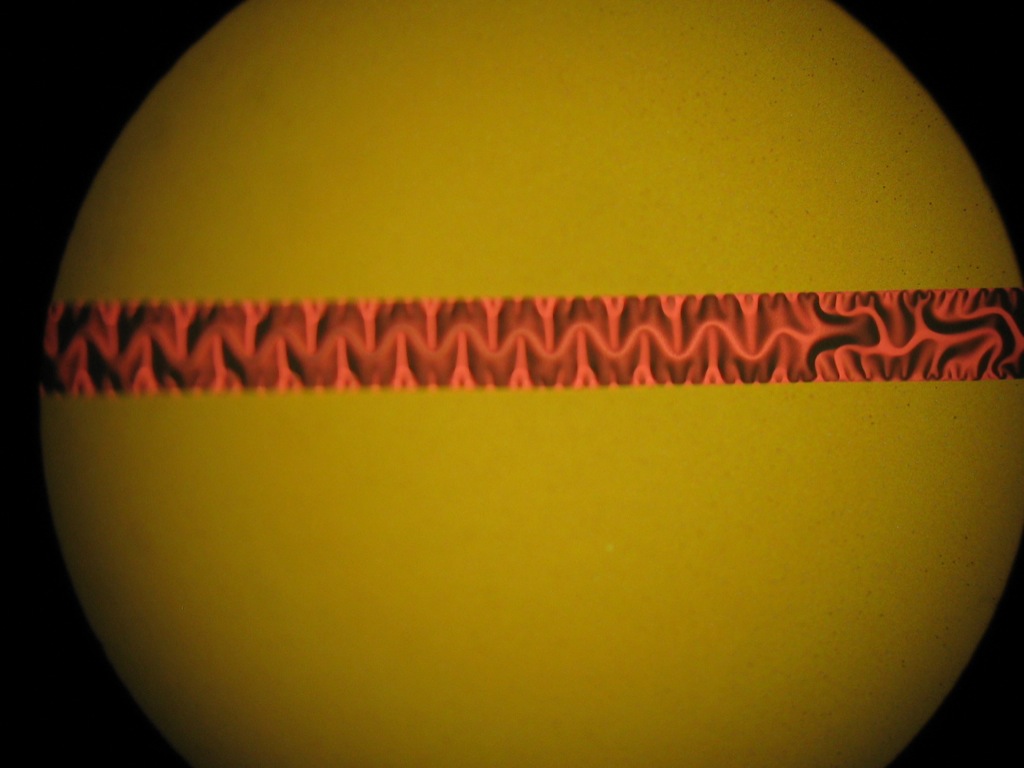
2- “Pinholes” (or very large pores) appear over substrate after RTP. These are just barely visible in these photos, but are obvious under microscope. They don’t seem to exist in the membrane.
30/50/30:
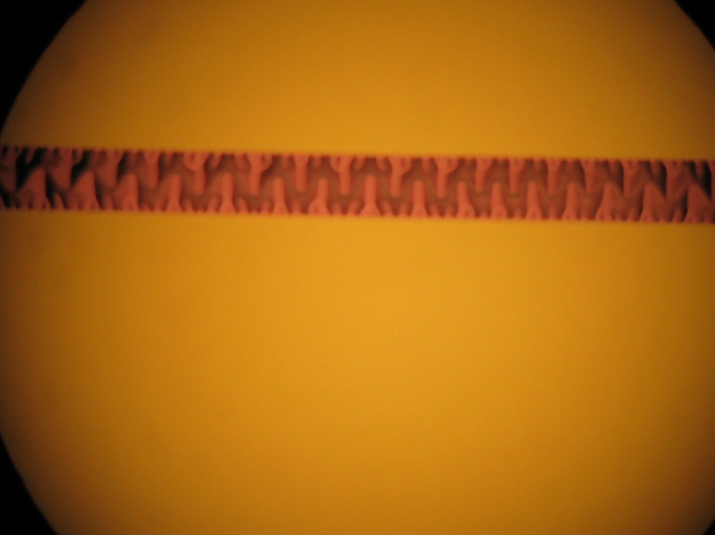
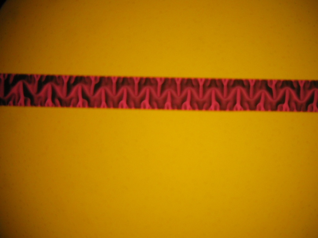
30/50/30 NSN post RTP post nitride strip (large pores/pinholes over substrate)


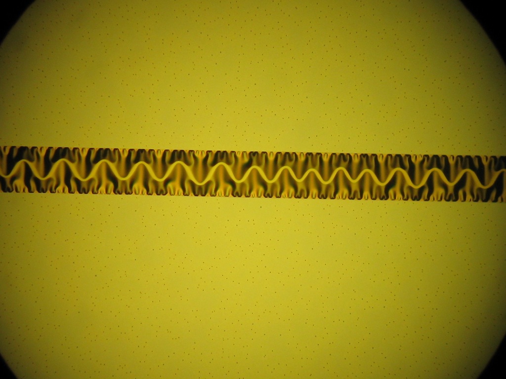
30/100/30:


The pore sizes and porosities that I calculated from these TEMs are different from those that Joe found.( NSN stacks with different Si thicknesses ) Most notably, the 30/100/30 NSN stack porosity is ~10% compared with Joe’s ~17%.
From inspecting various TEM and SEM images, it seems that the membranes on the SEPCONs prepared in this post have a large number of pits/voids that are nearly through pores, but not quite. Joe RTP several TEM grids at a time in the susceptor. Each SEPCON wafer was split and RTPed one half at a time. One guess, if we increase RTP temperature or soak time when processing 1/2 to full wafers we might get closer pore sizes to those found by Joe.
Next I looked at cross sections of the 30/100/30 NSN wafers to get an idea of morphology as well as determine any difference in thickness before and after RTP. (Spoiler- it gets thicker)


30/100/30 post RTP with nitride
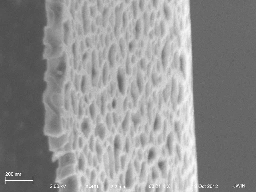
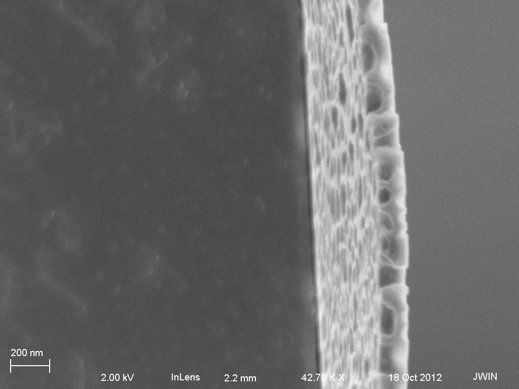

So the a-Si film thickness increases from ~90 nm to ~120-140 nm.
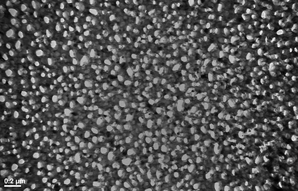
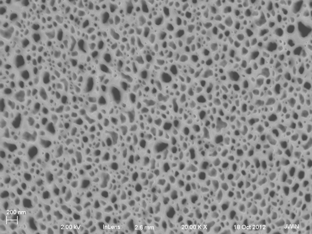
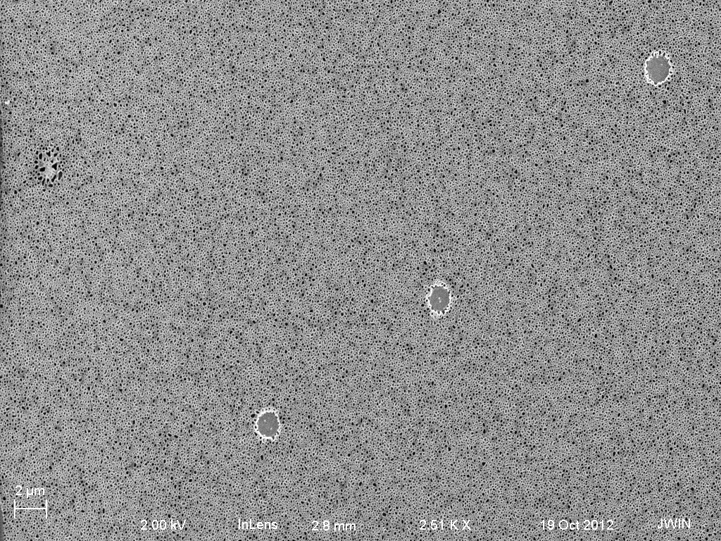
I also wanted to include some SEMs of the “pinholes” over the substrate:

Good job! One question, have you calculated that the increased thickness is in accordance with your porosity if we assume the mass conservation and the density doesn’t change?
I have not done that calculation. I’ll let you have the honor Joe!
These are interesting results. It’s great to get some confirmation that the pnc-Si layer does actually thicken during the anneal. This was the only explanation that made sense, but it’s good to see it directly in the images.
Some of the TEM images have an odd look to them. Are films this thick difficult to image or do they charge? Sharper images would probably help in the interpretation of the tremendous amount of structure in these films.
If the film goes from 90nm to 130nm, that would imply a porosity of around 30%. I think this is a reasonable estimation from the looks of the cross sections. By the way, how were the cross sections taken? Cleave through the membrane or was the FIB involved? This is also important in interpreting some of the structure.
It is unfortunate that the SIN is so compressively strained. This is the cause of the wrinkling and the “pinholes”. The pinholes are caused by the buckling of the nitride during the anneal, and loss of planarity and containment of the Si. These features may have an affect on yield, depending on whether they ever touch the edge of a membrane. If you annealed BEFORE the etch, I suspect the membranes may end up being more flat, but those “pinhole” features will kill the yield. If we could find conditions where these features do not occur, I think it would make the material far more reliable to manufacture.
What are your thoughts on device yield and membrane strength? It would be great if we can make devices out of this material on a consistent basis.
Thanks and good work Josh!
As for better TEM images, I could dip them in BOE to strip any native oxide. I imagine it is more difficult imaging thicker films, but I haven’t had much experience with with either thin or thick ones.
I made the cross-sections simply by breaking (cleaving just breaks the chip into pieces) the SEPCON chips. It’s really pretty easy to find an area to image.
The membranes seem strong, but again, I don’t have much experience with thinner SEPCONs. The yield was high. Maybe 70-80%?
It is true that it becomes harder to image when the membrane gets thicker. A high quality TEM requires sample thickness less than a few hundreds nanometers if I remember correctly. It also can be seen that it is not monolayer structure when the silicon film gets thicker and that’s why the silicon crystals look so dark in thick membranes.
Membrane 30/50/30 seems very porous. When I zoomed in the TEM image, I found those pores seem not open through and it seems there is something there. I’m wondering is that from the contrast or is it residue nitride?
Also I would suggest doing a longer annealing at 1000C or maybe at higher temperature and see whether the result is in accordance with our experience.
Just for your information. I have made one wafer for Krishanu and that wafer has NSN stack with 30/25/30 structure. I annealed that wafer first and then etched it. From what I can recall the pinehole density was quite high in that wafer both in free-standing membrane and the substrate. I forgot which pattern was that wafer.
I doubt there is anything over the pores, since this texture is too sharp. This is the background noise in the CCD that get exaggerated by the contrast setting. I’m fairly certain that the membrane itself has a high degree of stigmatism, but it’s hard to tell. Since this is the thinner sample, I think it should be possible to get a better image – might be worth asking Karen to try, or use Brian’s scope.
When you say 70%-80% yield, is this just the number that are unbroken or the actual number of completely pinhole-free (optical inspection) and usable Sepcons? I’ve seen wafers with all the membranes intact have poor final yield due to pinholes. My concern is that it only takes 1 pinhole that touches the membrane, and the device has to be scrapped.
Thanks!
Sorry I didn’t mention in the post, but the 30/50/30 pores look “cloudy” or “grainy” because there were no usable TEM grids so Charles broke out the membrane onto a 5nm nitride TEM window.
My 70-80% yield estimation is not based on a very thorough inspection, but what I did see through the microscope was either broken in a big way, or intact. I don’t recall seeing any pinholes in the actual membranes. That said, I think it would be a very good idea for me to inspect one of these wafers with Charles or JP to make sure I’m characterizing things in the accustomed manner.
Yeah, the detail about the 5nm SiN is important and explains some of the morphology. Is it possible this SiN texture was used to optimize the focus/stigmatism? The Si and the edges of the pores seem oddly fuzzy to me, which makes interpretation more difficult.
It will be interesting to get detailed yield data to understand the feasibility of this process. Since the pinholes appear to be substrate driven, I doubt you will find any on the open membrane areas. My main concern is the area of the substrate right at the edge of the membrane, and if a pinhole that forms in this region can grow onto the membrane edge and create a defect. Even a rare occurrence can have a strong effect on yield, since there is a lot of linear edge on a SepCon.
Thanks!