ALD ladders of SiN chips
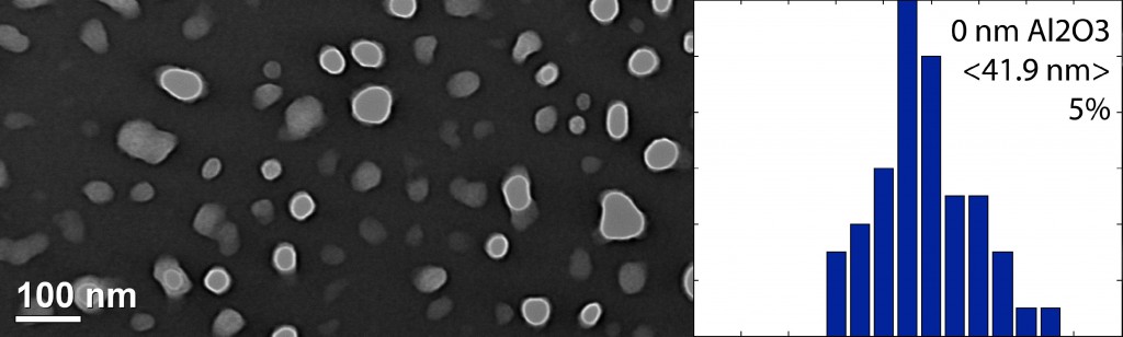
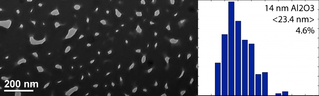
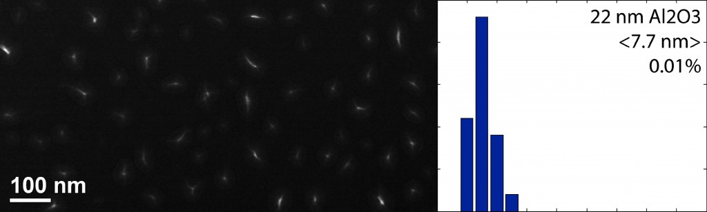
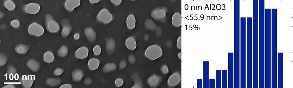
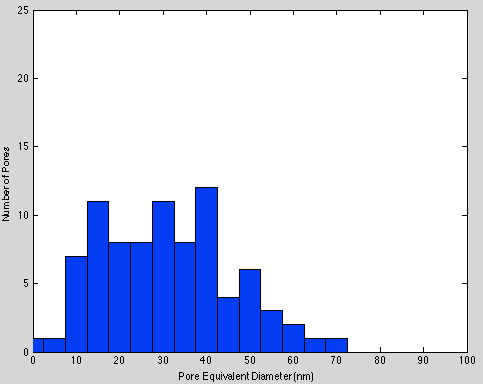
In all of the below graphs, the x-axis has the same scale for easy comparison (-10 nm to 80 nm diameter). The Y-axis varies from plot to plot, but since we care more about pore density than actual numbers of pores, I have left these numbers out. Here is an example full plot with MATLAB’s axis labels:
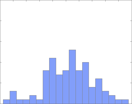
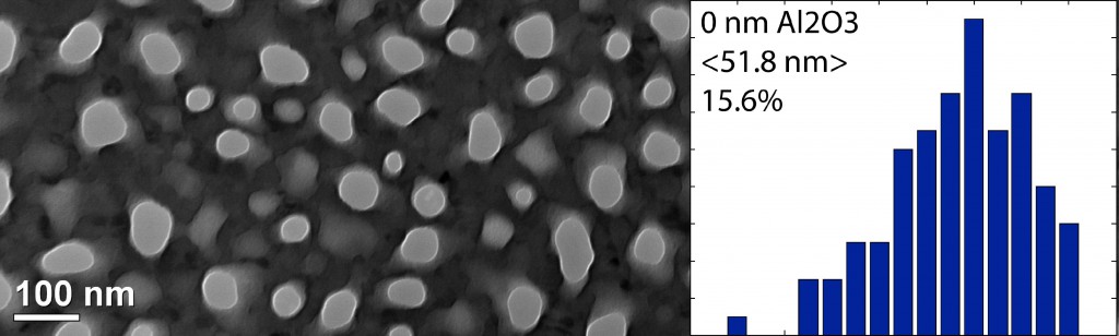
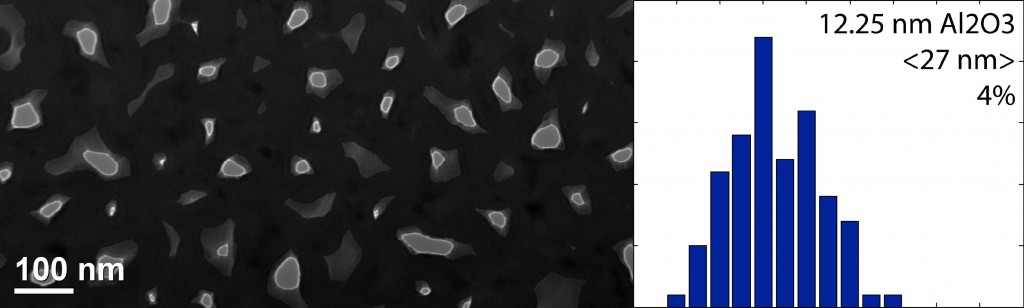
Wafer 1070 (SiN):

Note that the scale bar in the next picture is a little different from the other images:
Wafer 1081 (SiN):


Here, for comparison, are the expected values (blue, based on known deposition rates for alumina) vs. the actual measured depositions (red). Note that the x-axis values have changed, and that the y-axis is the same for all figures (this is different from the inset images):
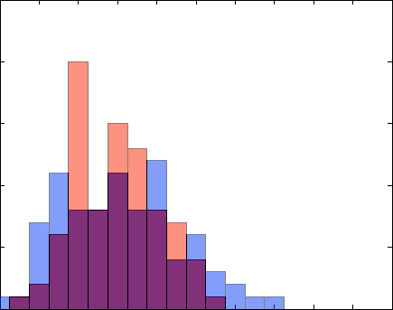
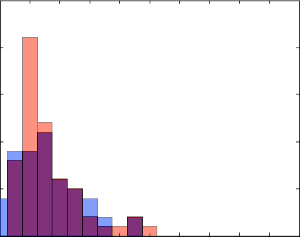
Blue is expected occlusion, red is the actual occlusion.
Unnecessary (and seizure inducing) .gif dramatization:

Wafer 1084 (SiN capped with pnc-Si):

I presented similar data for my qualifying exam. The salient figure:
