July 2015 NPN lift-off update
Summary
The CEIS project ended in June, and I am summarizing the last few weeks of activities below by Josh and me. We did a little more work on reducing the SU-8 film stress through the processing conditions. We also succeeded in obtaining smooth poly-Si films in the RIT SMFL. We made a few test wafers with this coating and had Rogue Valley deposit 50 nm of nitride on them to attempt lift-off with the RIT poly-Si. Josh applied pnc-Si on one of these and transferred the nanopores with RIE. Our attempts at lift-off with this NPN film were not successful in that we still observed tearing of the NPN upon removing it from the wafer after the XeF2 etch due to stiction. The hope had been that the RIT poly-Si would result in some residue left behind after the XeF2 etch and this would reduce the stiction force. Unfortunately, this did not prove to be the case. Finally, we repeated the procedure that Josh used ~2 years ago for making the microporous nitride nitride using another one of the test wafers. We found that this membrane could be successfully lifted-off even though it showed evidence of sticking to the substrate similarly to the NPN after the XeF2 etch was complete. This serves a good reproduction of the results he obtained two years ago. So, the 50 nm thick nitride is strong enough in the microporuos form but not in the nanoporous form to survive lift-off. We believe the reason for this is that the microporous membrane larger areas of contiguous, non-porous nitride membrane (on the order of 3 µm spans between adjacent micro-pores). In contrast, the NPN has merely 10’s of nm between adjacent nanopores. This led us to think that the next logical step would be to produce an NPN where the nanopores are transfered only in regions defined by a microporous pattern. This and other recommended next steps are discussed below.
Recommendations:
- Improve the tensile strength of the NPN by creating a microporous pattern through which the nanoporous are transferred into the nitride film (i.e., create a sub-scaffold of non-porous nitride). This should alleviate damage to the NPN during separation from the substrate and decrease the film stress mismatch between it and the SU-8 scaffold.
- Use thinner SU-8 struts to better match the etching times of clearing the windows to clearing under the struts. This would require a chrome mask for the SU-8 lithography, which would also improve the scaffold repeatability and quality.
- Use dissolvable photoresist layer to cover the center of the window areas to make the etch process more uniform between the open-window and SU-8 strut regions.
- Use thicker poly-Si in combination with smaller windows to prevent open areas reaching the substrate surface during the etch of poly-Si under the SU-8 strut regions.
- Incorporate holder device into XeF2 etch process to eliminate manual handling of LO samples.
- Use thicker nitride layer.
- Use higher tensile stress nitride.
- Use nitride as base under poly-Si (rather than thermal oxide) to reduce stiction forces.
Recommendation Discussion:
Unfortunately, none of the attempts we made to mitigate the stiction-related damage to the NPN membrane during lift-off were successful in eliminating the issue. The key issue lies in increasing the tensile strength of the NPN membrane. This can be done is several ways:
- Use of sub-scaffold of non-porous nitride by transferring the nanopores only to a micro-porous pattern.
- Increase its thickness, which will require development effort on how to obtain effective nanopores transfer.
- Perhaps using a high tensile stress LP-CVD nitride coating will help. This may also alleviate some the wrinkling observed due to the film stress mismatch between the NPN and the SU-8 scaffold.
- Moving to finer features for the SU-8 scaffold may also be helpful for a couple reasons. One is that the poly-Si etch would be more uniform. Presently, the majority of the open windows are etched free with the first XeF2 pulse, and the remaining 7-9 pulses (for a ~1 x 1 inch sample) are required to remove the poly-Si trapped under the 10 µm wide SU-8 struts. Finer features will require a chrome mask, but this would result in a cleaner scaffold pattern that what we get with the acetate-based mask now. It would likely be useful to move to smaller open windows (maybe 25 µm square) to reduce the spans of NPN membrane that can sag down to the underlying surface during the etch.
Another mitigation strategy is to minimize the stiction force. We thought that by going to the RIT poly-Si, this would perhaps result in a thin residue layer being left on the surface of the oxide that would reduce the stiction force. Unfortunately, this turned out not to be the case. Other approaches that would reduce the stiction force are:
- Perhaps using a layer of SiN under the poly-Si would be better as its surface charge would the same as the NPN membrane. This layer could perhaps even be applied in the LP-CVD tool at RIT just prior to depositing the poly-Si (they are done in the same tube of the tool).
- Other methods that would leave a surface with roughness on the scale of ~ 1 micron. This is challenging. since the top of the poly-Si much be smooth a the level of nm to create the pnc-Si and subsequent nano-porous transfer. One thought is to simply apply the nitride layer directly to the wafer surface and etch into the wafer Si rather that a poly-Si sacrificial layer. Etching the single crystalline silicon results in a roughened surface that will presumably display much lower stiction forces with the NPN membrane. The issue is that the XeF2 etch becomes approximately an order of magnitude longer. This could be reduced, however, if thinner strut features are used for the SU-8 scaffold.
The other approach that was only briefly explored in this project is to add a fixture to the XeF2 etch tool that enables the lifted-off NPN membrane to fall or settle directly onto a hemodialysis module as it is released from the substrate. We found that hanging the sample upside-down over a capture module did not result in the membrane falling from the surface, presumably because of the high stiction forces. There are possible options along this line that are worth exploring if the above mentioned ones are not fruitful. One thought is to not use an SU-8 scaffold, and simply place the wafer sample over a capture device that has a support scaffold (perhaps made from PDMS). Perhaps by using a surface treatment on the capture device, the NPN membrane would be attracted to this surface and lift-off as the XeF2 etch progresses. There may also be advantages to designing the geometry of the capture device to facilitate staged etching across the surface of the sample (e.g., preferentially direct the etchant flow at the center of the sample, such that the corners don’t curl up prior to the middle portion’s etch being complete).
Repeat test of microporous nitride lift-off
As a final test in the project, we decided to test LO of a nitride membrane patterned with ø3 µm pores (hexagonal close-packed, 6 µm pitch) using one of the thin wafers as opposed to the thicker ones that Josh used in his original work of microporous nitride LO. We chose one of the wafers with the RIT poly-Si that had not been coated with the amorphous Si and capping SiO2 layers, and patterned it with the micropores using the Drytek REI tool. We applied the SU-8 scaffold (100 µm square) using Josh’s original conditions. A 1 in2 sample was tested for LO and we found that the membrane appears to be sticking to the oxide surface upon completion of the XeF2 etch, but it does not suffer any damage once it is separated from the surface an transferred to a holder. This indicates that a key contributor to the NPN membrane damage is its lack of contiguous, non-porous regions in the nitride film to provide strength over the lengths scale of 10’s of microns.
This observation made us think that the next logical step to try would be to create a “sub-scaffold” for the NPN membrane by transferring the nanopores in a micropore pattern. This could be accomplished by applying and patterning a photoresist over the pnc-Si layer prior to performing the nanopores transfer RIE in the Trion etcher. This would limit the nanonpore transfer to the micropore regions.
Smooth poly-Si at RIT
Our initial tests early in the year with wafers that had be coated with poly-Si at RIT’s SMFL proved to be unacceptable for the NPN transfer process because of a roughened poly-Si surface. We initially solved this issue by sending wafers to Rogue Valley to be coated with their poly-Si, which had a much smoother surface (compared to original SMFL poly-Si tested with AFM). After discussing the LP-CVD process with the SMFL process engineers, it seemed that using a lower deposition temperature would likely result in a smoother poly-Si surface, so this was attempted. Deposition on the original wafers was done at 630 °C, and there exists a recipe for 610 °C. The lower temperature does result in a lower deposition rate (~6.5 nm/min vs ~10 nm/min for 630 °C). One wafer was run through a 110 min. deposition (target of 750 nm layer), and optical micrographs are shown below in Figure 1 that illustrate the surface roughness difference between this one and original ones, at least in a qualitative sense. Note that in the micrograph of the 610 °C poly-Si, the defects seen in the left portion of the image are included simply to show that the microscope was focused on the correct plane. These defects are very rare on the surface, and the surface smoothness was so good that it was generally difficult to keep the microscope focused on the surface without some type of surface defect for reference.
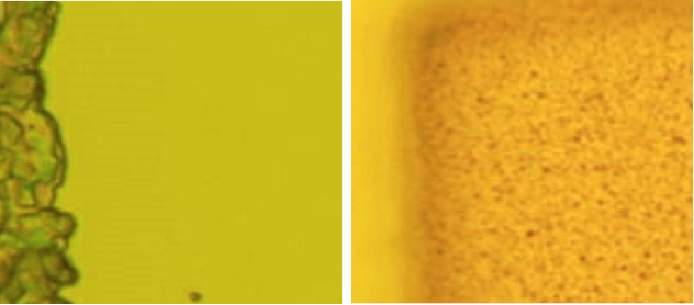
Figure 1: Optical micrographs taken at 50x and focused at the poly-Si surface of (Left) poly-Si deposited at 610 °C and (Right) original, 630 °C poly-Si layer. The 630 °C layer has a 50 nm SiN film on top with unsuccessful nanopores transfer, and the SU-8 scaffold strut is visible (out of focus) in the left portion of the micrograph.
Based on this promising result, we deposited poly-Si on three of the double-side polished wafers after growing 100 nm of dry thermal oxide. It was further recommended to us that running a shorter, “warm-up” deposition in the LP-CVD can improve both the deposition rate and smoothness of the poly-Si film, so we ran a single test wafer first for a 15 min. deposition (target 100 nm film). The test wafer had a 200 nm TEOS-based oxide layer, which may not be ideal for measuring the poly-Si layer using the Spectramap instrument, but the measurement came out to 101 nm. We ran the three device wafer through the same recipe with a deposition time of 107 min (target 750 nm film). The Spectramap measurement yielded a thickness measurement of 975 nm, which indicates a deposition rate of 9.1 nm/min, or ~33% faster than the warm-up run’s. The deposition rates should be investigated further at a future time using the same oxide base layers to ensure reliable Spectramap measurements.
We had these wafers coated with 50 nm of the low stress nitride by Rogue Valley and tested them in the LO. The hope had been that the SMFL poly-Si has enough trace contaminants in it to mitigate the strength of stiction after this layer is etched away by XeF2 so that the NPN membrane could be lifted-off without damage. In testing of NPN LO with one of these wafers, we found that the damage was qualitatively similar to that seen with LO tests of wafers with the Rogue Valley poly-Si layer.
SU-8 Processing to Reduce Stress
In addition to the annealing treatments, I tried modifying the SU-8 processing conditions to minimize film stress. Reading various sources including MicroChem’s data sheet and websites for microfab centers, it seems that SU-8-3000 film stress can generally be reduced by using longer bake times and starting form lower temperatures, particularly for the post-application drying (PA) bake and the post-exposure (PE) bake. I think these are primarily geared toward much thicker coatings (e.g. 50 µm) than what we use. In Table I, the three sets of conditions are summarized: those typically used in our studies, the “lower stress” one, and the original one that Josh used two years ago when doing the microporous nitride lift-off work. A test wafer was coated with SU-8 according to the lower stress protocol and yielded a measured film stress of 1.2 MPa, tensile, which is significantly lower than ~2.1 MPa for the typical conditions. Likely, the most important changes are regarding the longer PE bake time at lower temperature followed by a slower ramp up to the final PE bake temperature of 95 °C.
Table: Summary of processing conditions for the SU-8-3000 scaffold.
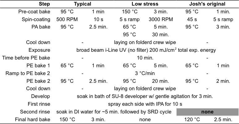
There are very few differences between our “typical” and Josh’s original processing conditions except that no water rinse is used at the end of the development step, and this seems to be particularly beneficial for enabling good wetting of the wafer surface with BOE to strip off the thin layer of oxide that was applied to improve SU-8 adhesion. In the cases where we used water rinse after the IPA rinse, we found that the surface was very hard to wet in the BOE solution, which results in a much less certain etch rate. Over-etching the NPN/SU-8 system is of concern since BOE does etch nitride (at a fairly slow rate). Also, we have found that if we strip the oxide too aggressively the SU-8 scaffold will delaminate from the surface, presumably because the BOE eventually undercuts the thin oxide upon which the SU-8 is sitting.
Other SU-8 scaffold patterns
It was thought that use of scaffold patterns with smaller open area windows and perhaps a square vs. hexagonal might reduce or eliminate the tendency of the NPN membrane to tear when being lifted from the oxide surface after completion of the XeF2 etch. We tried lift-off with two square patterns: 50 x 50 µm and 100 x 100 µm openings, both with 10 µm wide struts. Qualitatively, there did not appear to be much improvement when using these patterns in terms of the observed damage to the NPN LO membranes.