Journal Club – Oo et al, 2016 – A nanoporous gold membrane for sensing applications
Paper: Oo2016
Supplementary Info:Oo2016SI
Abstract:
Design and fabrication of three-dimensionally structured, gold membranes containing hexagonally close-packed microcavities with nanopores in the base, are described. Our aim is to create a nanoporous structure with localized enhancement of the fluorescence or Raman scattering at, and in the nanopore when excited with light of approximately 600 nm, with a view to provide sensitive detection of biomolecules. A range of geometries of the nanopore integrated into hexagonally close-packed assemblies of gold micro-cavities was first evaluated theoretically. The optimal size and shape of the nanopore in a single microcavity were then considered to provide the highest localized plasmon enhancement (of fluorescence or Raman scattering) at the very center of the nanopore for a bioanalyte traversing through. The optimized design was established to be a 1200 nm diameter cavity of 600 nm depth with a 50 nm square nanopore with rounded corners in the base. A gold 3D-structured membrane containing these sized microcavities with the integrated nanopore was successfully fabricated and ‘proof of concept’ Raman scattering experiments are described.
Figures:
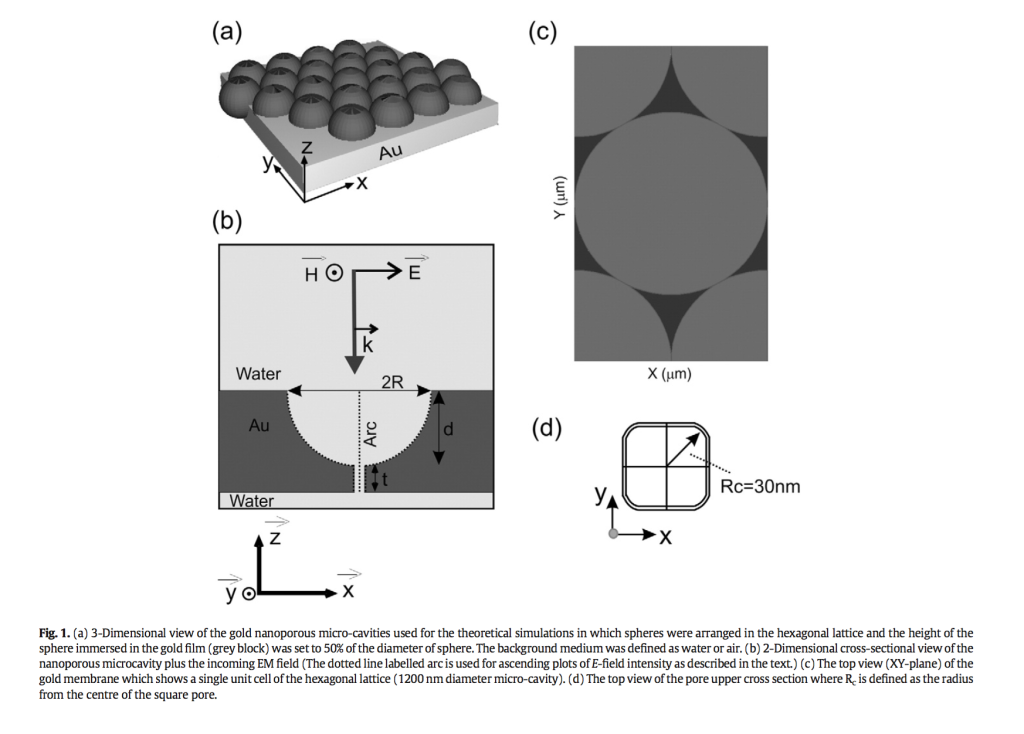
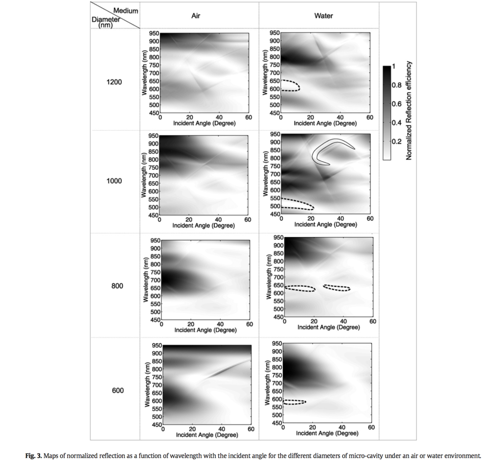
Fig. 3 The cavity is simulated in different environments (water and air) and there are zones of low reflection efficiency (eg absorption), attributed to surface plasmon resonance for these conditions. There are optimal angles for striking a resonance.
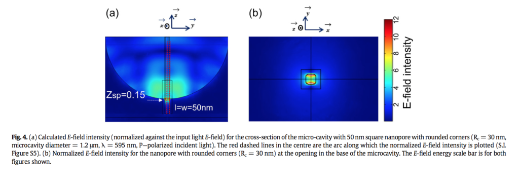
Fig 4. E field intensity is localized inside the pore. The square shape with rounded corners throws more of the E-field intensity into the center of the pore, rather than to edges.
Supplemental video shows a simulation of where the electrical field enhancements are in the microcavity, tending around the area of the FIB pore, across a variety of wavelengths.
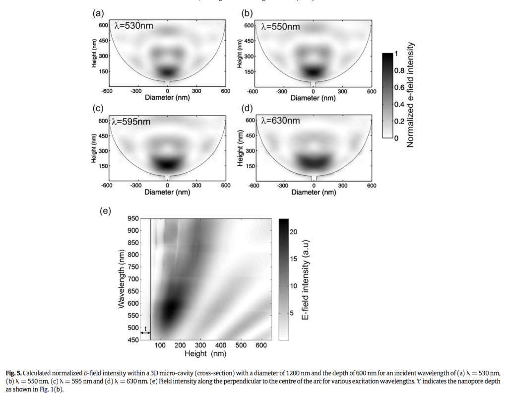
Fig. 5 Normalized E-field intensity across the cavity (relative strength instead of absolute strength).The strongest E-field enhancement occurs in a range between ~525-600 nm, 100-200 nm off of the surface.
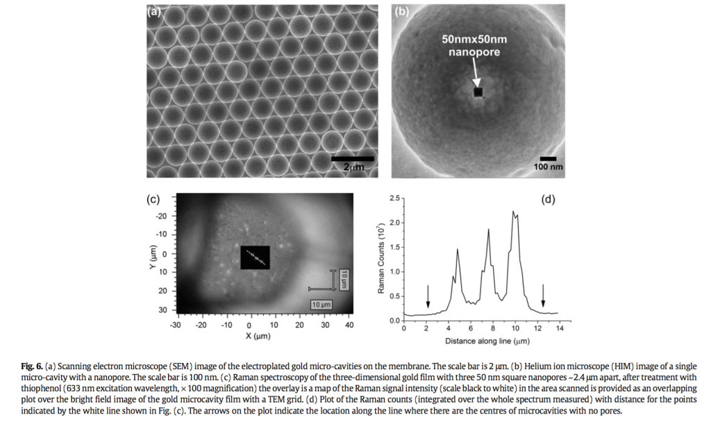
Fig 6. Physical data! The packed spheres seem to have done the job of creating repeating microcavities, though the inner surfaces appear to be rougher than the simulated smooth surfaces. The actual increase in Raman counts (baseline = ~0.5/3=0.16e7) appears to be 9-12x (integrated over the whole spectrum).