RTP Ramp Rate Effect on 6W Bias pnc-Si Stack Increases Pores Size Slightly
Purpose: We want to know the effects of the RTP process on pore size, pore density for the biased films coming out of the AJA. I believe that the RTP ramp rate is important for forming bigger pores. Some work (Joe Qi Thesis) has indicated that the pores come out more circular as the wafer is heated at a faster rate. Currently, a 5W bias is used to deposit a film stack.
Methods:
1. Film stack Deposition
- Deposited 40 nm Si + 20 nm SiO2 on top of 100 nm SiN film from Rogue Valley (6” wafers).
- Recipe: pnc-si-00-40-20.
- Bias was 6 W (12% of 50 W max rate).
- 30 RPM rotation enabled.
- Tool was cleaned right before deposition. 4 wafers were deposited in 4 separate runs.
2. RTP of film stack to form pnc-Si
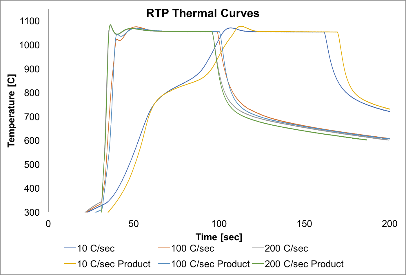
- 3 wafers were heated at different ramp rates (10 C/s, 100 C/s, 200 C/s) in an Argon ambient to produce pnc-Si.
- The RTP tool was warmed to 800 C for 5 minutes using the standard warmup recipe. Wafers were unloaded at 500 C, and then placed on an aluminum plate to cool at 300 C. Wafers were loaded immediately at 200 C, and the recipe was started when the thermocouple read 100 C.
- 10 C/s, 100 C/s appeared normal, 200 C/s had a small defect centered on the contact point with the thermocouple.
3. Sample Separation
- Wafers were stripped of the 20 nm SiO2 layer with a 10:1 BOE dip, and subsequent SRD.
- Wafers were cleaved to produce 4 treatment conditions from each ramp rate step (12 samples total) and scribed with their names.
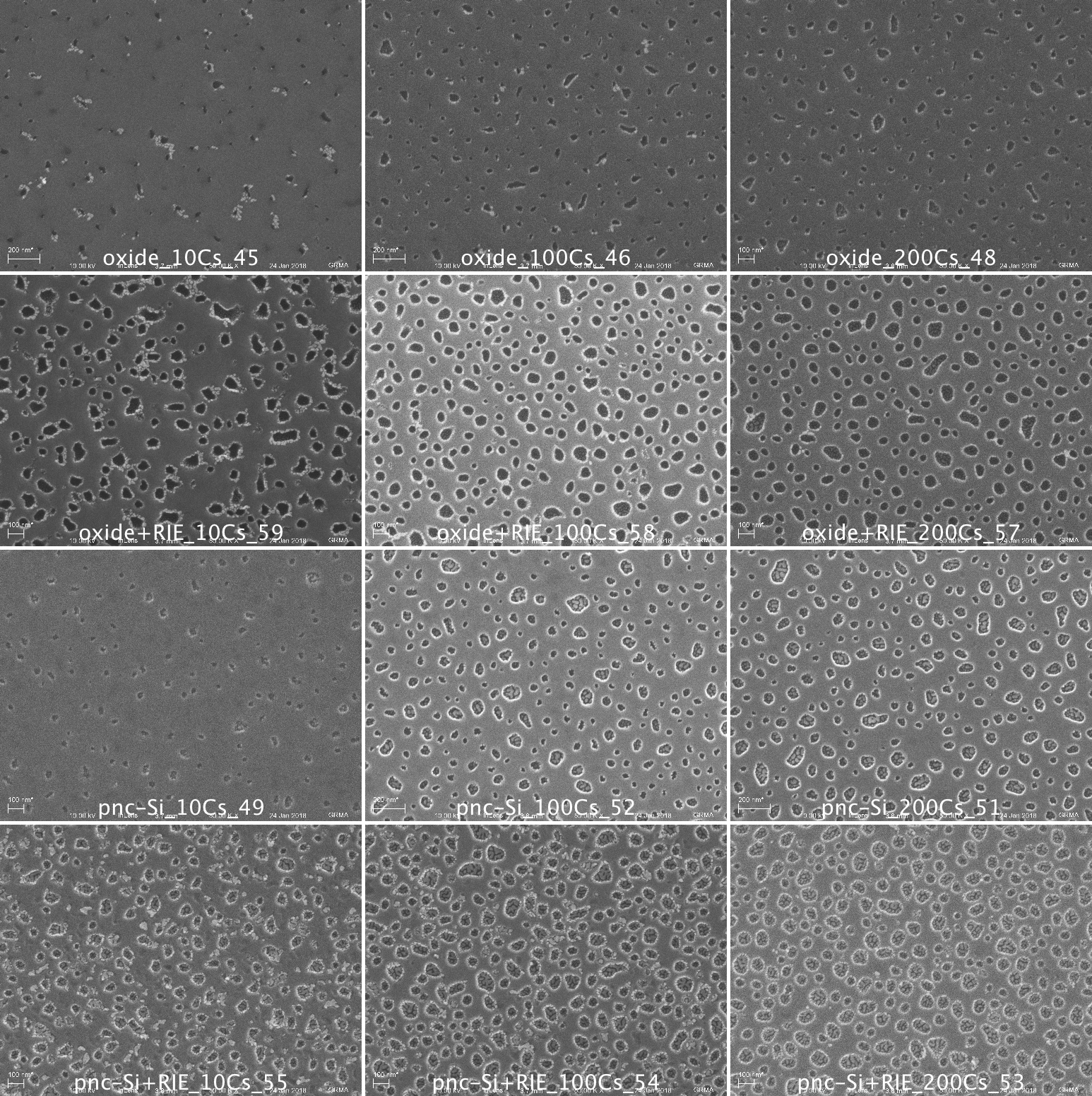
- Pnc-si is the material natively out of the RTP (pnc-Si). Pnc-Si + RIE is material etched into the underlying SiN (NPN). Oxide is pnc-si that has been oxidized using a thermal furnace (pnc-Si). Oxide + RIE is the oxidized material that is etched into underlying SiN (NPN)
4. Oxidation of pnc-Si
- Wafer pieces were oxidized in RIT’s Tube Furnace
- SMFL 100nm Oxide growth recipe 462 overnight, Tube 4
5. Reactive Ion Etch
- Wafer pieces were etched to transfer the pore patterns into SiN
- Trion RIE had some plasma instability initially, but recovered over later runs
- Trion cleaned with a 10 min O2 and Ar plasma
- Seasoned for 30s with Etch recipe: 50 sccm CHF3, 5 sccm O2, 10 sccm Ar, 175 W
- 10 C/sec oxide+RIE and 100 C/sec oxide+RIE had plasma interruptions, but were etched for an appropriate time
- Oxide+RIE pieces were etched for 135 seconds, pnc-Si was etched for 94 seconds.
- Wafer edges appeared clear and mirror-like, and there is a blue central color to the wafers, indicative of successful etching.
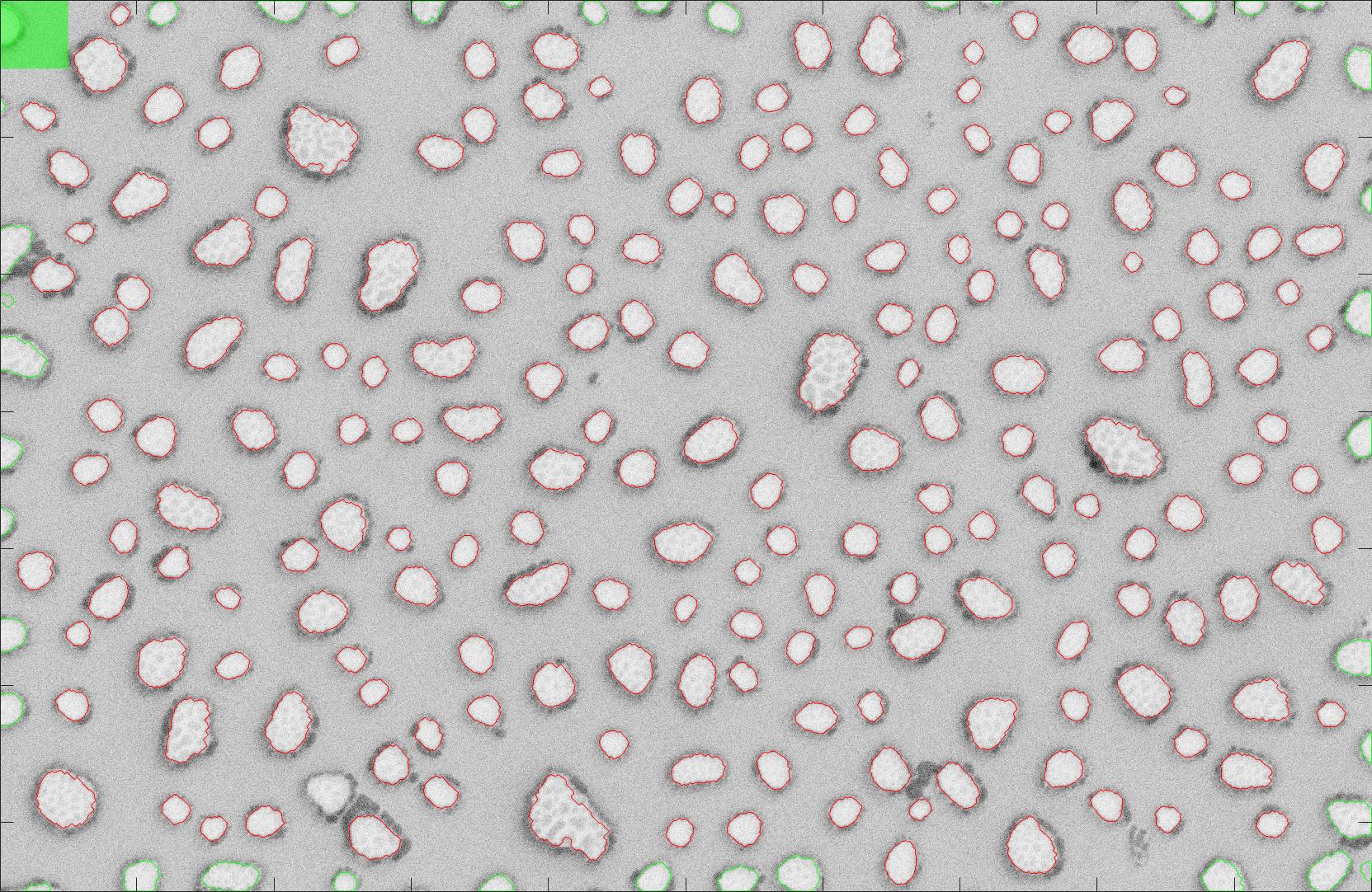
6. SEM imaging + Analysis
- Samples from the center of each wafer piece were cleaved and coated with 6 nm of Au using the Denton Sputterer (no rotation) in the URnano prep room.
- Samples were scratched centrally to denude them of gold in certain regions for imaging. 20kx, 50kx 100kx images taken.
- Pore histograms were calculated for some 50 kx images using the pore image processor software (MATLAB). Images were inverted using Fiji.
Results


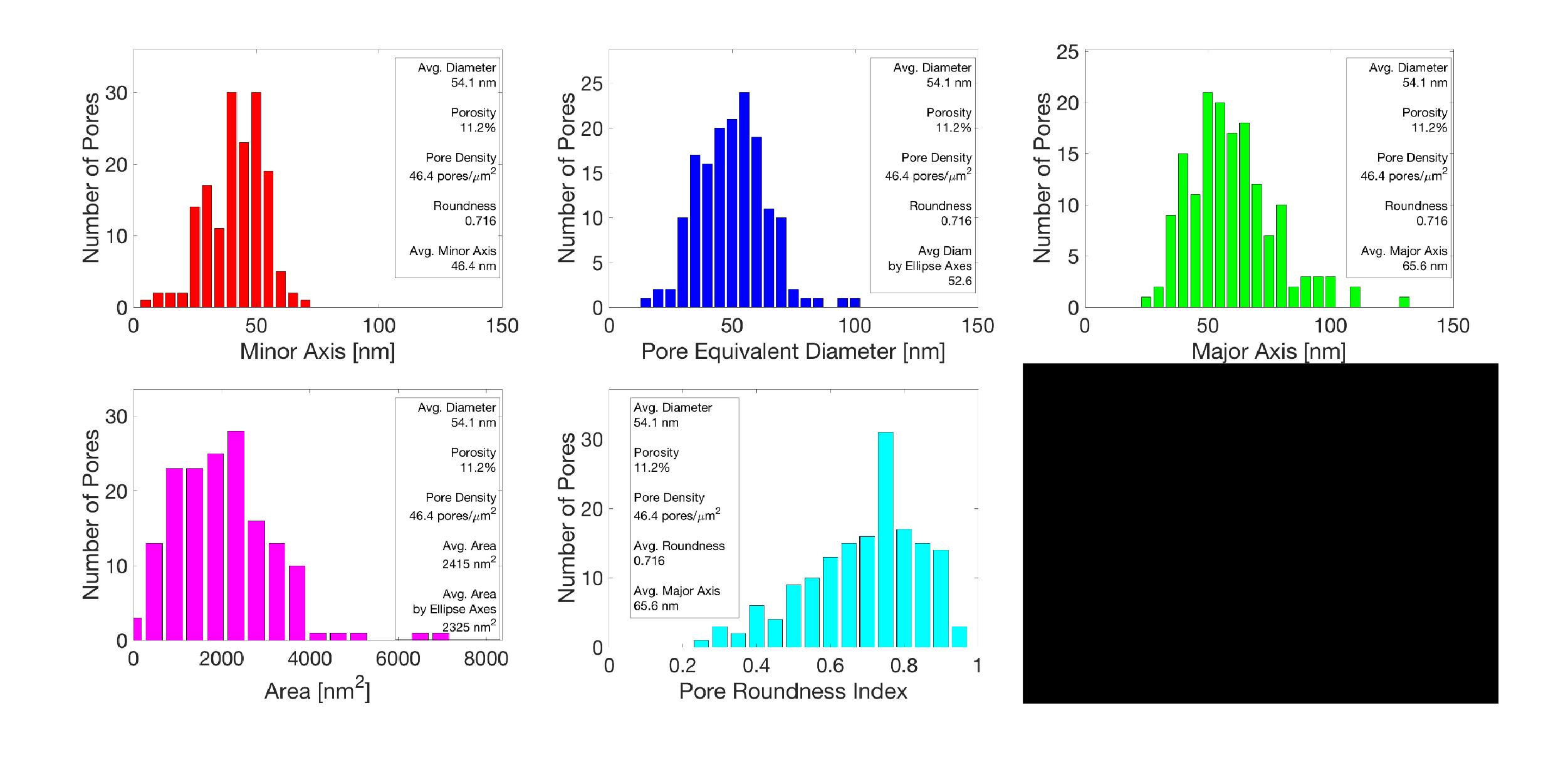

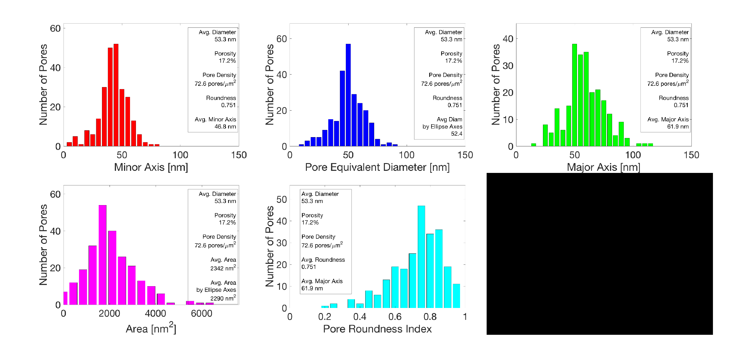
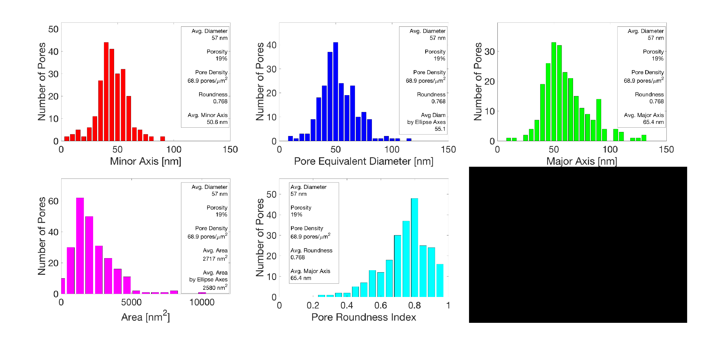
Conclusion: Heating up the stack 3x as fast as normal increased the average size of the pores by a few nanometers, but did not appreciably change the pore density. Lowering the ramp rate led to decreases in pore density, but the average size of pores was preserved. The circularity is not obviously different between the 100 C/sec and 200 C/sec conditions. Ultimately, the thermal stress defect of the faster ramp rate probably does not make it worth producing.