Fabricating 500 nm Channels in Silicon Wafers
Summary
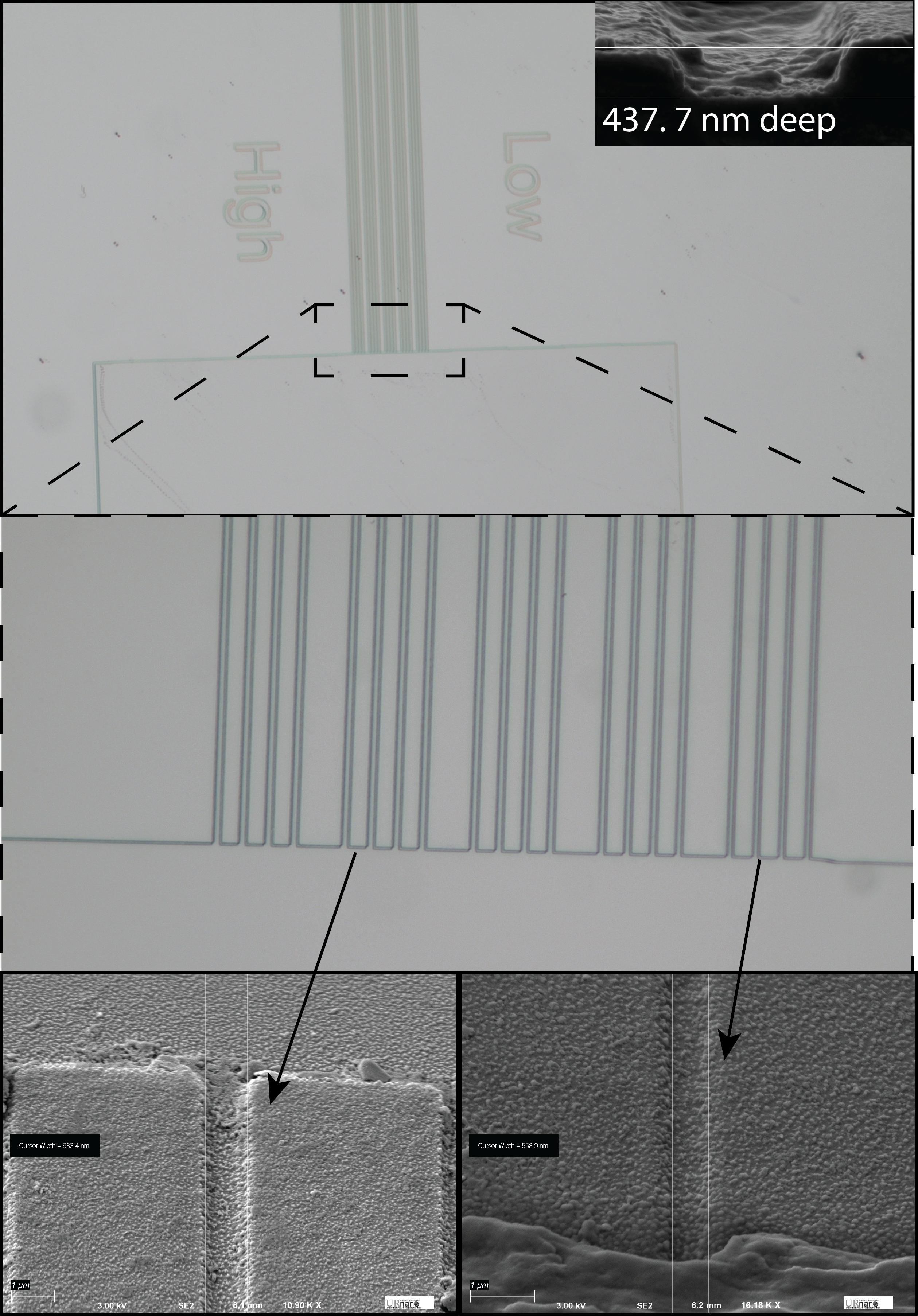
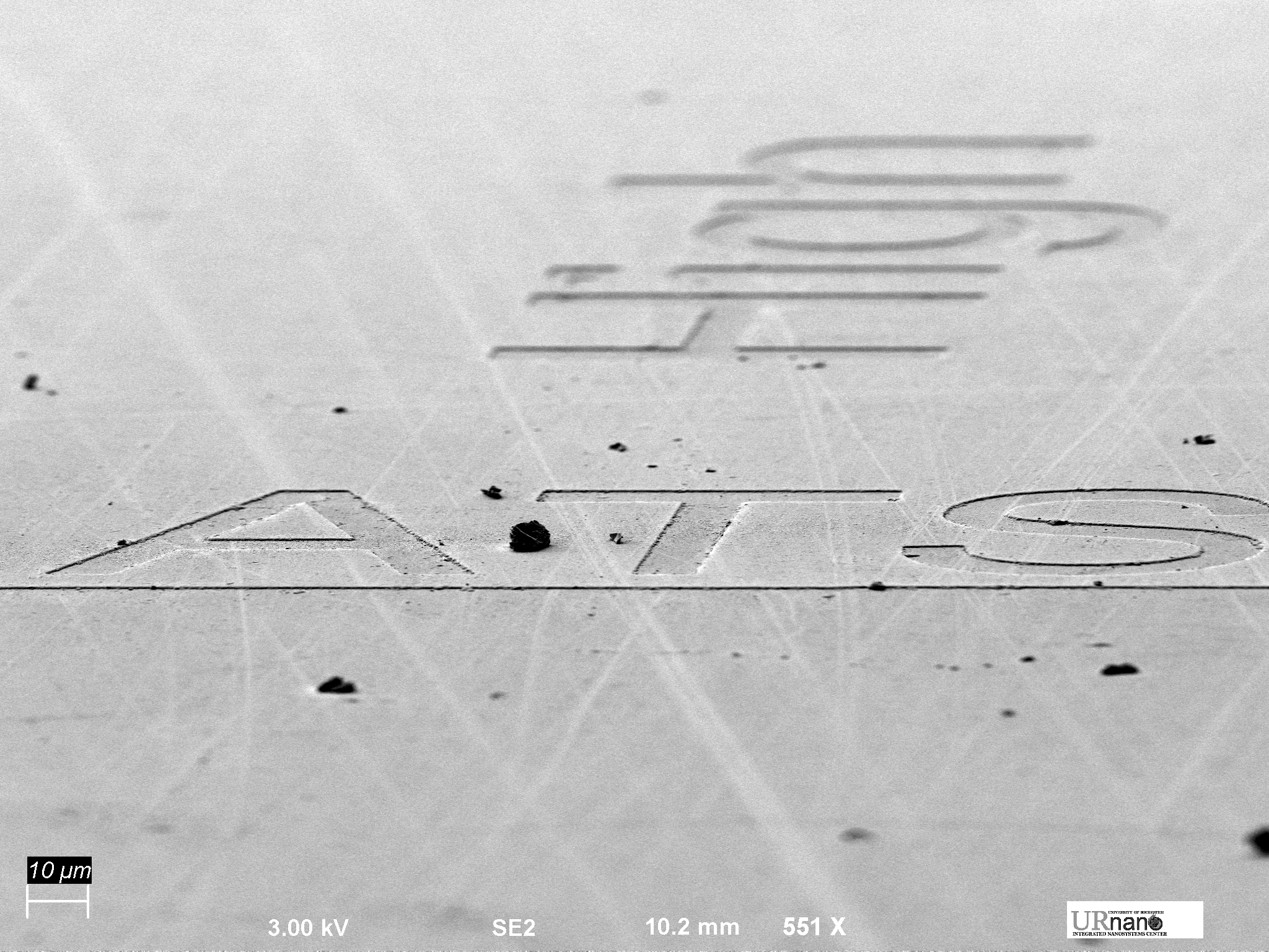
This post complements Fabricating 0.5 um Channels in Microscope Slides for Staph Invasion Assays. Challenges in the etch transfer process necessitated switching to a different substrate that had stronger selectivity. With that in mind, we set out to create 500×500 nm channels in silicon wafers for the bone invasion study. We had partial success (micron-sized channels, 350-500 nm deep) with slightly different coating protocols and exposure compared to the previous post, and there is some additional room for optimization in the etching.
Methods
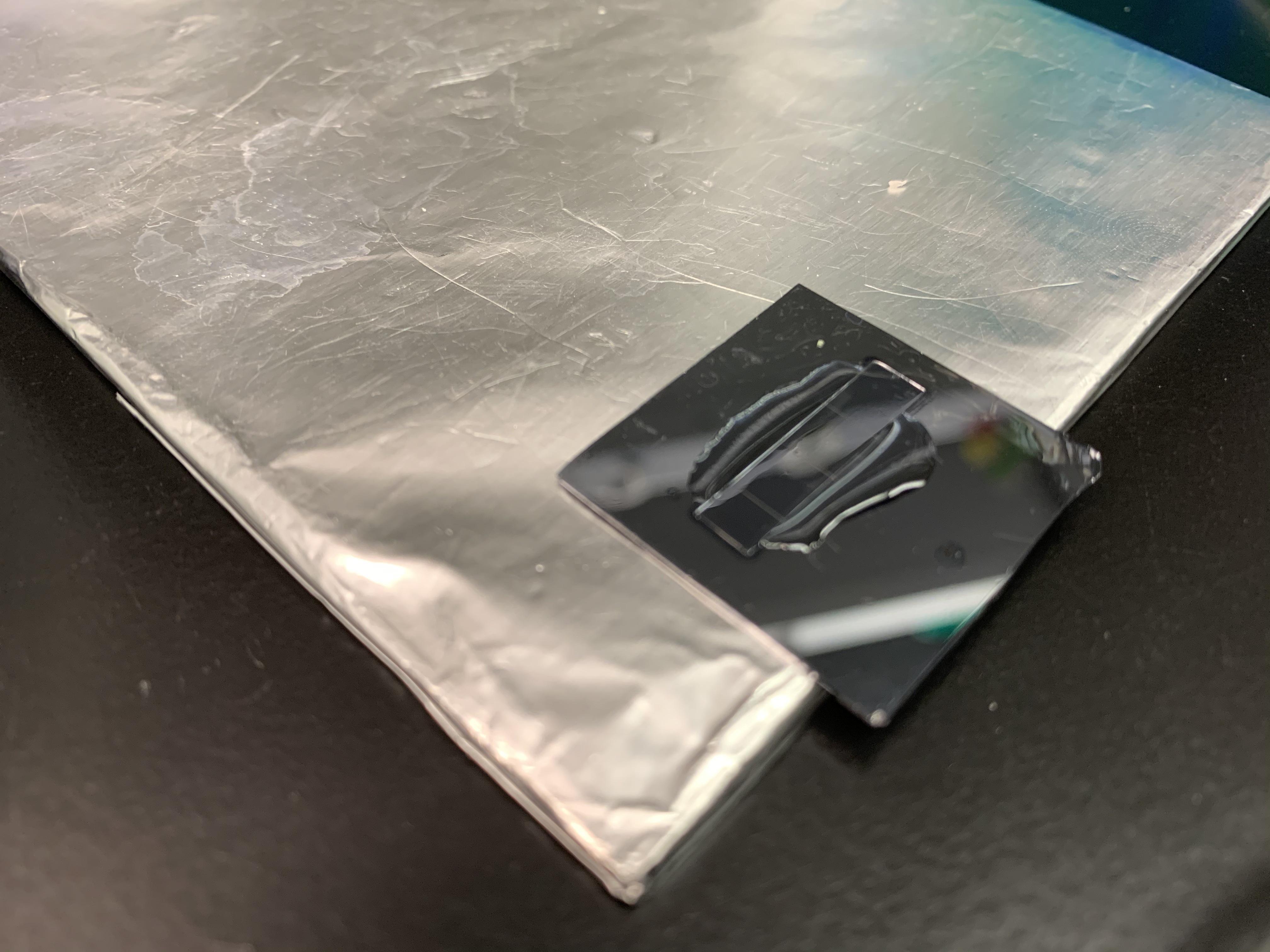
Cleaved double polished Si wafers were coated with P20/HMDS and Shipley S1805 using the following spin protocol:
- 5 sec @ 1000 RPM (add adhesion reagent or photoresist in this step)
- 50-60 sec @ 5000-7000 RPM
- This step controls the thickness of the photoresist, more photoresist produces a thicker mask, which can lead to a longer etching time. The downside is that the feature resolution is not as good.
- 5 sec @ 1000 RPM
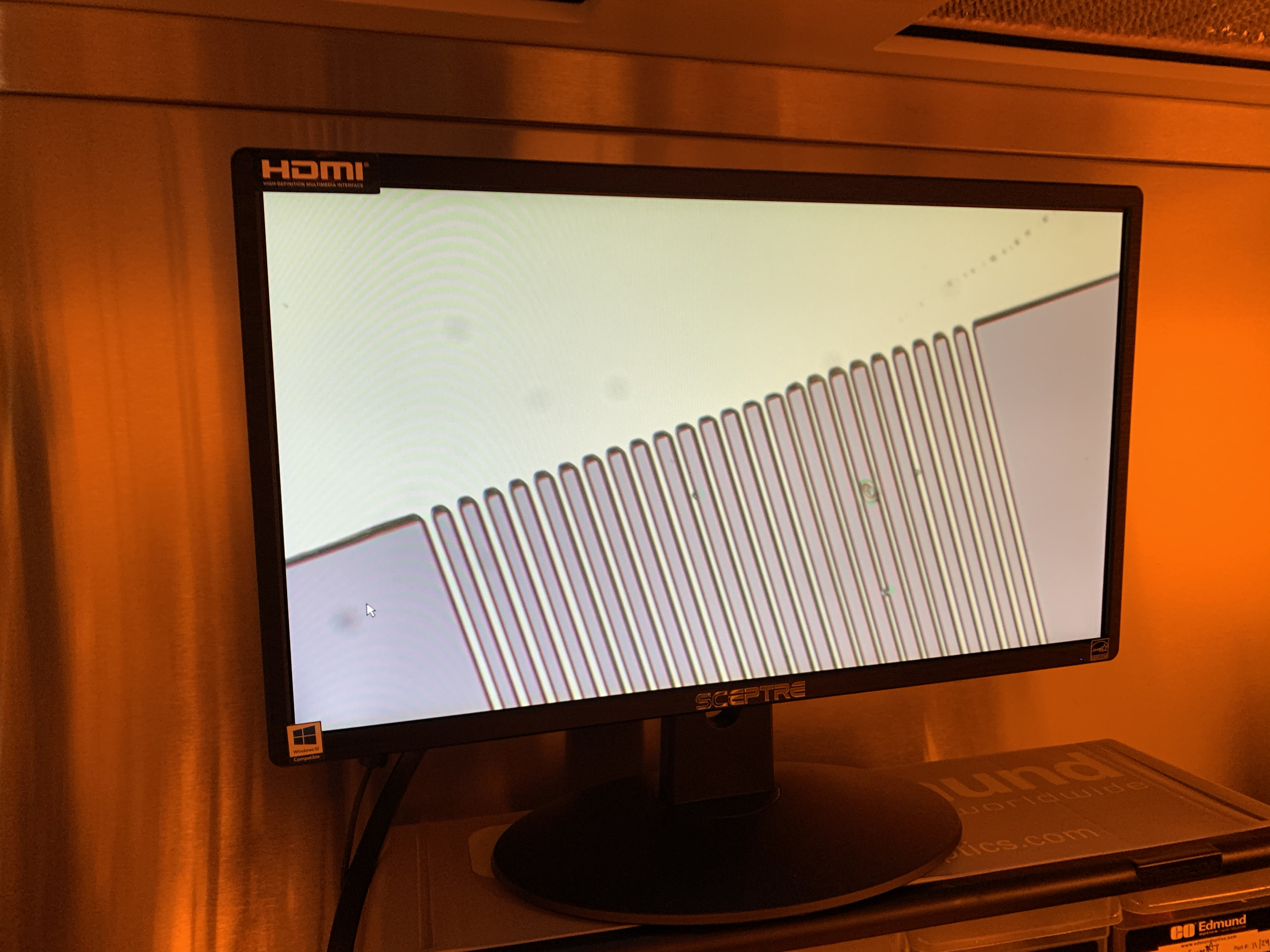
Coated wafers were then transfered to a hotplate and soft baked for 60 sec. Important temperature control is necessary, as we found that the temperature of the hotplate and cooling setup can drastically change the photoresist exposure characteristics.
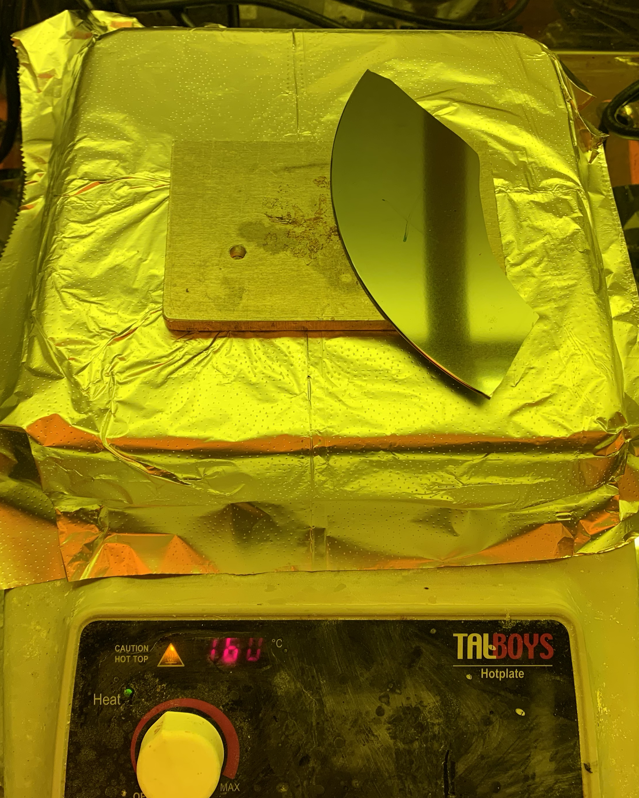
- Set the hotplate to 150C, use an aluminum block and a Si wafer to get consistent readings off of the wafer. Read with an infrared thermometer (90 C)
- A small experiment showed that 85-90C on the wafer will have exposures that develop properly in this configuration, but 102-110C on the wafer will not.
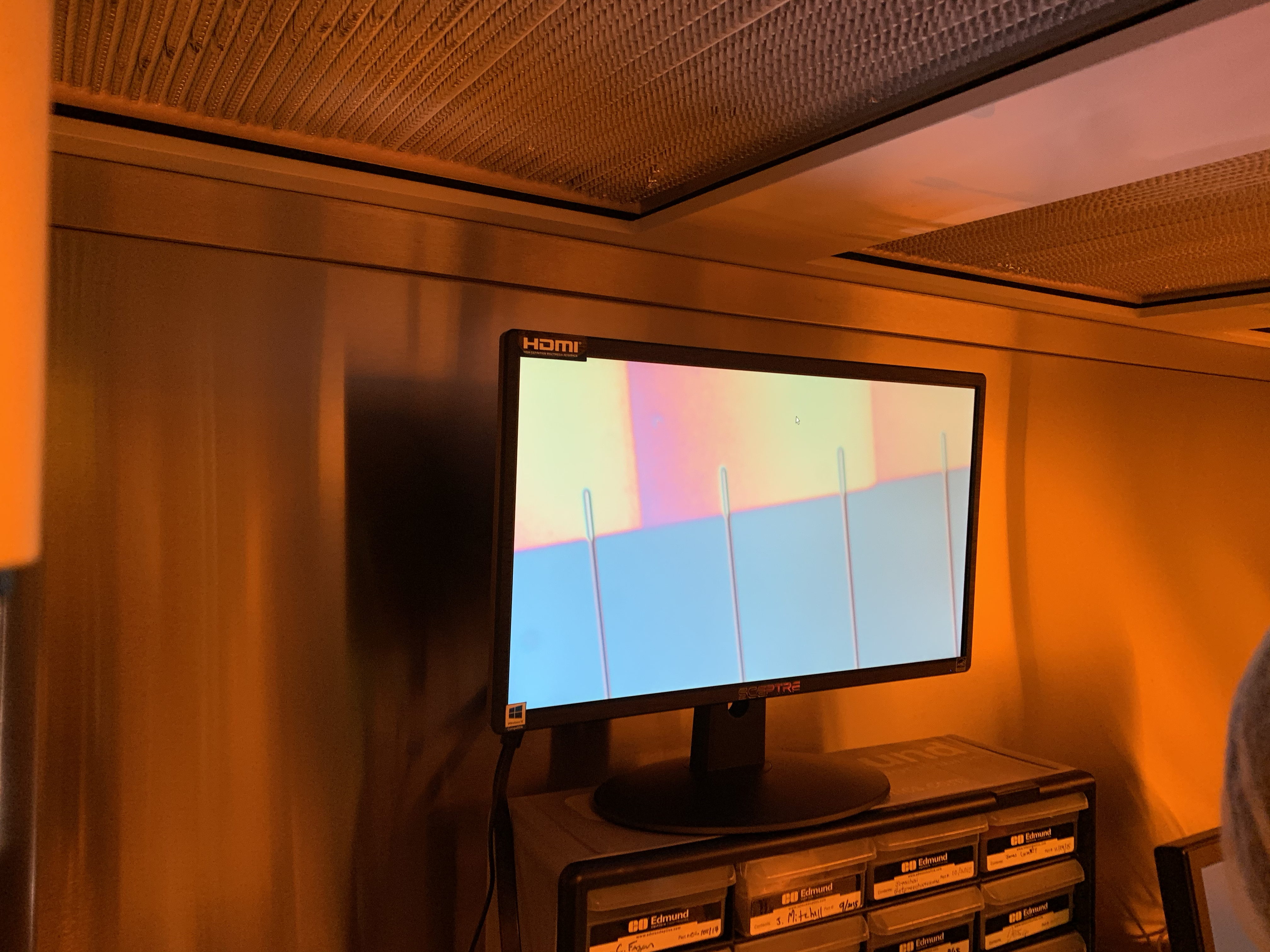
Coated chips were transferred to the laserwriter and loaded into the tool.
Using lens 5, the photoresist was brought into focus (Z ~= 1900-1950 um) for this thickness of wafer), and the following parameters were set:
- Filter: 1%
- Pos: 2 mm/s
- Write: 2 mm/s
- Vector Mode
- Planar autofocus correction (established M1, M2, M3)
We had designed in ClerWin a number of channels that are 2 mm long and 500 nm wide, grouped into bunches of 4 channels. These channels were then assigned into separate layers (5 layers, 20 channels total), and written at different exposure levels to produce a range of developed channels in the photoresist. The gain settings were often set from 0.3-0.7, or 0.2-0.4, or 0.25-0.35. The entrance pad to the channels was written with a different set of exposure settings (Filter: 3%, Beam-scan mode, 150 mJ/cm^2 dose) to broadly overlap with the channel entrances.
After exposure, exposed wafer pieces were developed in MF-319 for 30 sec using some swirling agitation and rinsed thoroughly with diH2O, then dried with the nitrogen gun. Finally, the wafer pieces were hard-baked on the hotplate for 180 seconds.
The patterns were then etched into the silicon wafer using the Oxford RIE and the following recipe
siSF6 recipe
- 10 sccm O2
- 40 sccm SF6
- 20 sccm CHF3
- 100 W
- 50-80 mTorr etch pressure
- Known to aggressively attack photoresist
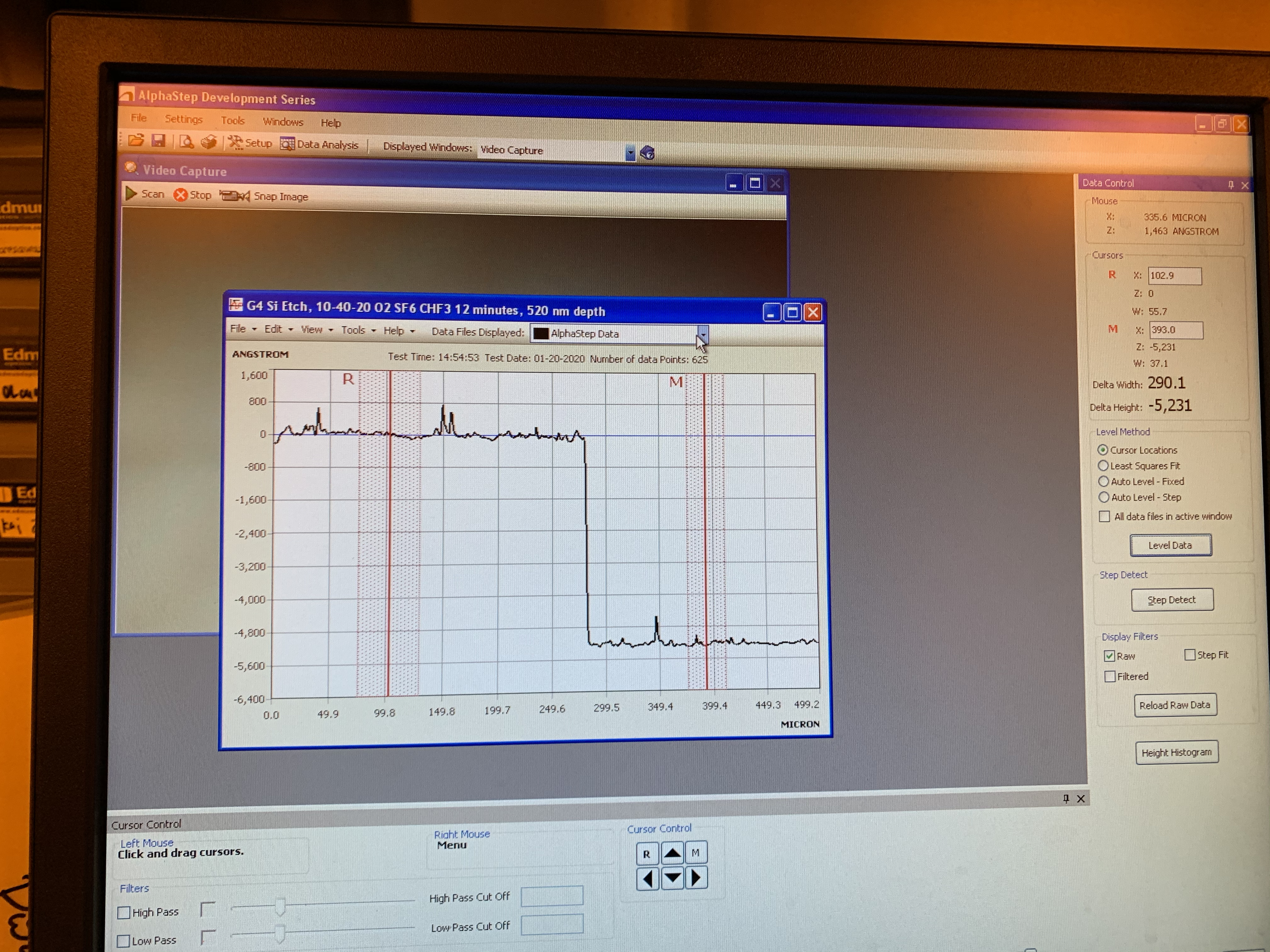
- 12 minute etch used to etch as much as possible into the substrate
Wafers were then cleaned with acetone, or a 100W, 100 mTorr, O2 plasma for 5 minutes. The plasma cleaning provides more consistent cleaning, and has does not have the potential to form residues on the surface.
Metrology was done on the pad areas of the pattern, or under SEM with 5-8 nm platinum coating.
Results