AFM of SiO2 film roughness
Dave did a series of 20nm SiO2 film depositions at different temperatures (constant bias) and gave them to me to AFM. I guess he wanted to see if film roughness changed drastically over the range of ‘room temp – 400C’ in order to investigate this as a potential source of pinholes.
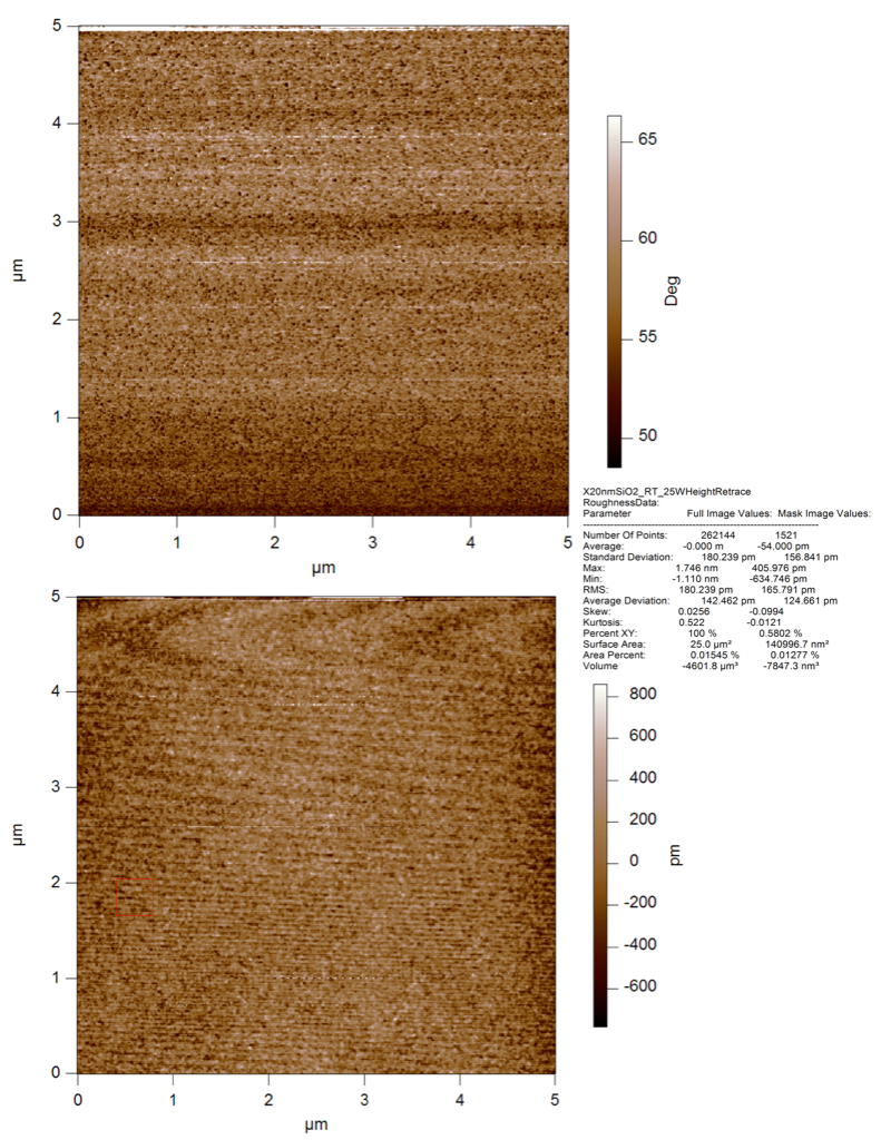
I used a new AC160 tip to acquire these images. I included that topography (top) and phase (bottom) scans. On the topography scans is a red box – that is the mask used to calculate the roughness. Roughness data is in the textbox.
The room temperature deposition:
The 400C deposition (I had trouble keeping the tip in reulsive mode – you can notice the phase hopping around a bit at the end (bottom) of the scan):

These both are really flat surfaces – a bit more than 1 Angstrom of RMS roughness. Also, the roughness didn’t increase significantly from room temperature to 400C. Dave made a couple of other temperature depositions, but I was having trouble with phase hopping again. I am not having good luck imaging silicon wafers. I wonder if the tip is building up charge…..I’m going to email Asylum to discuss.
Thanks Barrett. With all deposition processes, it’s very important to keep an eye on film roughness and refractive index, as this is a measure of the quality of the deposition recipe. We routinely use ellipsometry to measure the refractive index, however this technique relies on the assumption that the roughness is low, creating abrupt interfaces. The AFM is great confirmation that our films are indeed smooth and confirms that our ellipsometry data is valid. Your data indicates that the roughness is comparable to that of a bare wafer, which is a very good sign for us. I think Dave is going to ask you to make a similar measurement on a sputtered Si film, for additional validation of our recipe. Thanks again!