Problem with copper…
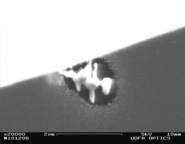
The SEM image shows an area at the very edge of a membrane. The bright region is the silicon wafer and I am looking down at it from above. The pinhole is the dark round region and the rest of the membrane is grey. Sitting inside the pinhole is the copper silicide “particle”.
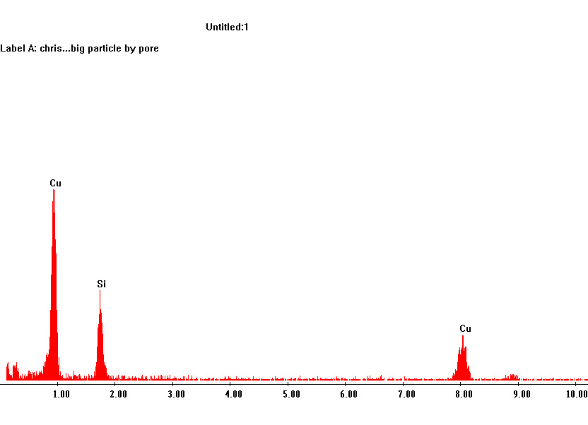 The EDX spectra is self-explanatory – the particle is made of copper and silicon. The silicon signal is not from the membrane itself, as it is too thin to generate a signal much above the noise level (and confirmed experimentally). Actually, having an ultrathin silicon membrane made this elemental analysis very easy due to the low background – an application we should keep in mind. This spectra indicates the Cu:Si ratio is 11:9, however copper silicide should be 3:1.
Anyway, the mechanism to explain this breakdown in the membrane is unclear, but it would be reasonable to assume that if we remove the copper contamination, this problem should go away. Interestingly, copper is the fastest diffusing contaminant in silicon (D~0.0001 cm^2/s @ 700C and still significant at RT), and this mobility probably plays a role in this process.
The good news is that we know all the process steps where copper could potentially be entering the system. The bad news is that it will probably take us a week or two to positively identify the source, and more time to develop a work-around. My first guesses for the copper source (in order of likelyhood) would be: 1) Sputter heater, 2) etching cell, 3) RTP or furnace
at RIT, 4) Contaminated EDP from manufacturer 5) Contaminated bath/chemicals
at RIT, 6) Source wafer contamination.
We’ll get started on fixing this on Monday, but JP and Dave just processed a wafer without the sputter heater (please confirm) that could contain a clue or two. I’ll try to check this out over the weekend.