Microporous Magnesium Fluoride Nanomembrane Becomes Stronger as the Film Thickness Increases
The title really says it all. I have been attempting to make a better cell culture substrate with the Magnesium Fluoride Films. Previous posts have shown the overall structure of the film, and now I am trying to quantify the strength with a burst pressure measurement. In order to make a direct comparison, I needed to utilize the same window/pore geometry, and only vary the film’s thickness. I used wafer PFI02 (120 nm silicon nitride, 0.4 micropores, 1:1 pitch, five 0.1×3 mm slots).
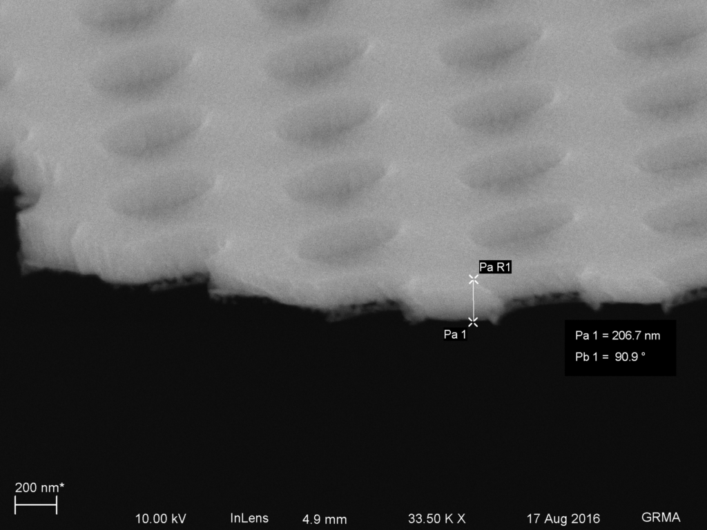
Here, I’m comparing a 50 nm thin film process (actually came out about 45 nm) to a 200 nm thin film process.
50 nm Process
- Evaporate MgF2 onto 0.4 micron pore, 12o nm thick Si3N4 substrates
- 250 C
- 2-3 Angstroms/sec
- Platen Rotation
- Etch with RIE, backside to remove Si3N4
- CHF3:O2 (90%:10%)
- 100 W Net Power
- 100 mTorr etch pressure
- Etch for 120 sec
200 nm Process
- Evaporate MgF2 onto 0.4 micron pore, 12o nm thick Si3N4 substrates
- 150 C
- The different temperature is to mitigate the larger overall amount of film stress generated by the thicker film
- 2-3 Angstroms/sec
- Platen Rotation
- 150 C
- Etch with RIE, backside to remove Si3N4
- CHF3:O2 (90%:10%)
- 100 W Net Power
- 100 mTorr etch pressure
- Etch for 120 sec
The burst pressures then are (slowly ramping up with N2 gas, ~1 PSI every 5 sec):
| 50 nm Process | 200 nm Process | |
| 1.12 | 6.98 | |
| 0.73 | 6.92 | |
| 0.82 | 9.43 | |
| Average [PSI] | 0.89 | 7.78 |
| Std. Dev [PSI] | 0.20 | 1.43 |
Increasing the thickness 4-5x improved the burst pressure strength by ~8x. There are yield improvements too; many of the broken chips for the 200 nm process had more windows than that of the 50 nm process. Here I only got 3 chips for each treatment, but I processed 9 chips for the 200 nm process and about 20 chips for the 50 nm process. This data suggests that I am on the right path to make more robust cell culture membranes.
Greg: Can you directly pattern the micropores into MgF2 with photolithography and RIE?
BTW – We use Si-rich, non-stoichiometric SiN (so not Si3N4).
Thanks for the reminder that the film is non-stoichiometric – SiN, not Si3N4. Will update post to reflect this fact.
You could pattern the micropores, but I have yet to find an effective RIE that attacks the MgF2. I’m sure it exists somewhere, but my own experiments show very little etching of the film with CHF3-based chemistry. Maybe we could wear it away with an Ar plasma over a long time? It will all come down to the selectivity – what sort of photoresist thicknesses are we working with nowadays (1-3 um)?