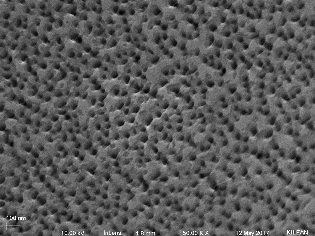
Better SEM images of 75 nm membranes
All of the images are from the same 75 nm NPN four-channel chip.
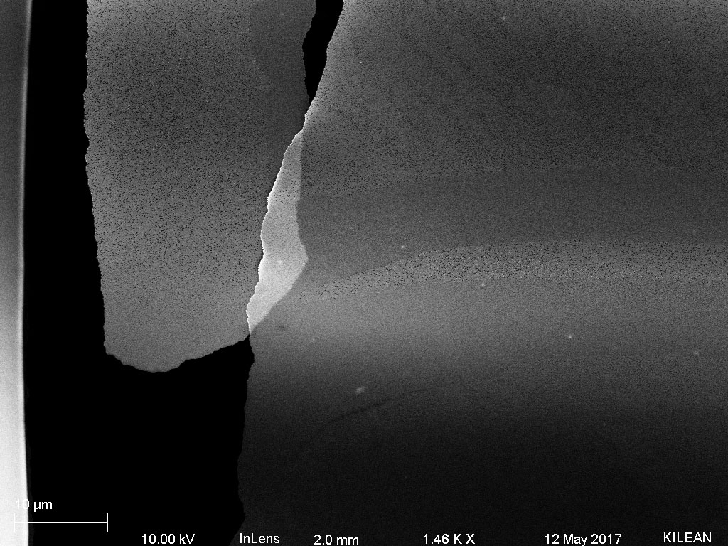
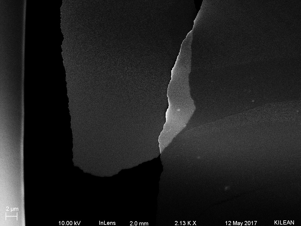
The first images shows the edges from the backside of the chip, showing how flat it is (without the oxynitride present on the top side). There is a crackle-like texture but the third image, which shows the corner of the membrane and two of the sloping sides, shows the same texture on the etched channel walls, meaning the texture is from the gold-platinum deposition (40 s). At least it isn’t a feature of the backside of the NPN.
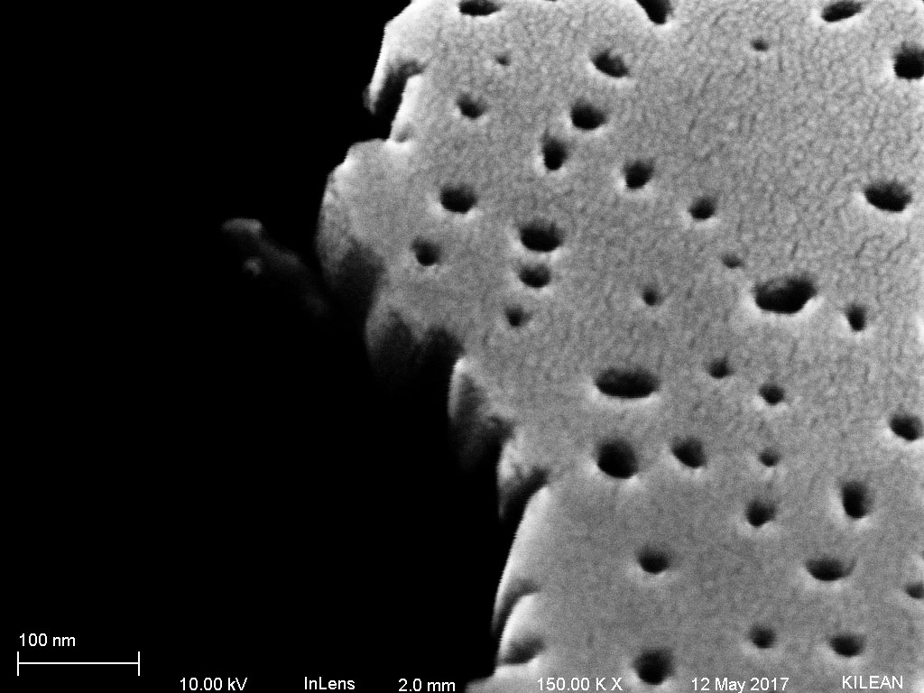

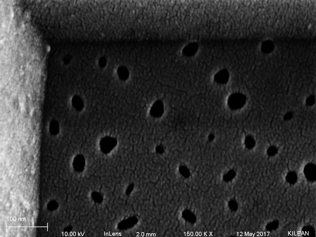
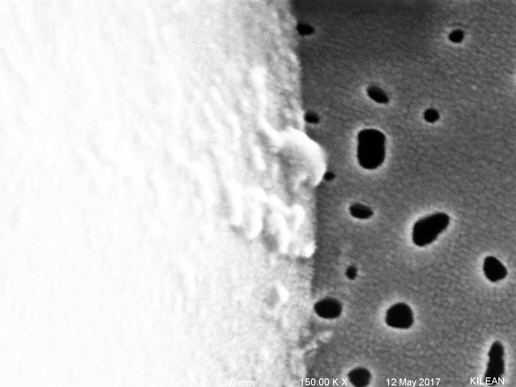
The next three images show the pores as they appear on the backside.


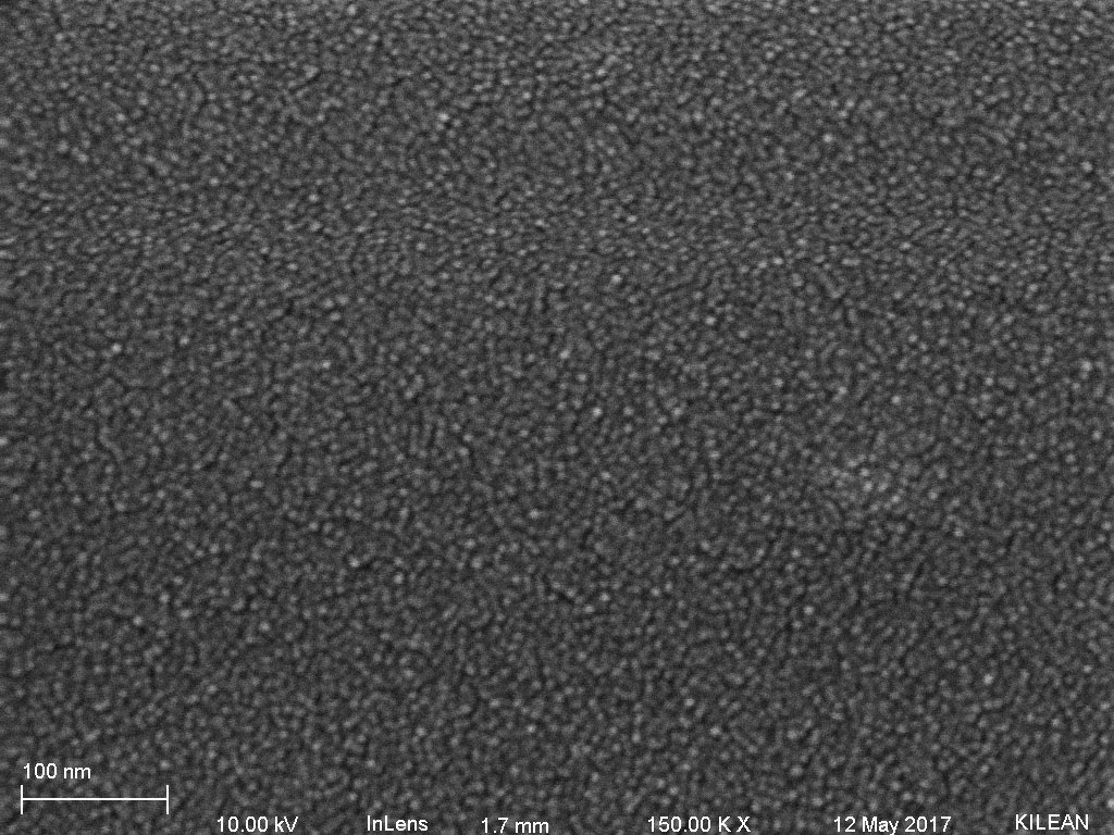
This next image is of the backside of the bulk silicon wafer. There is a texture similar to everywhere else but without the crazing. This could be due to the difficulty in focussing on nothing.
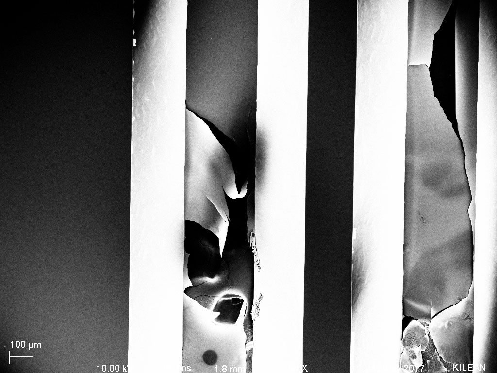
Now to find the top of the membrane. I found a nice little curl where the membrane was adhered to the sample holder.
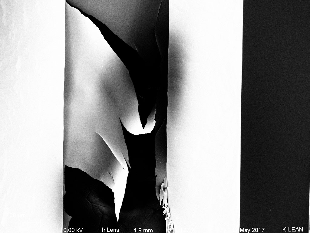


The final four images show two membranes overlapping.

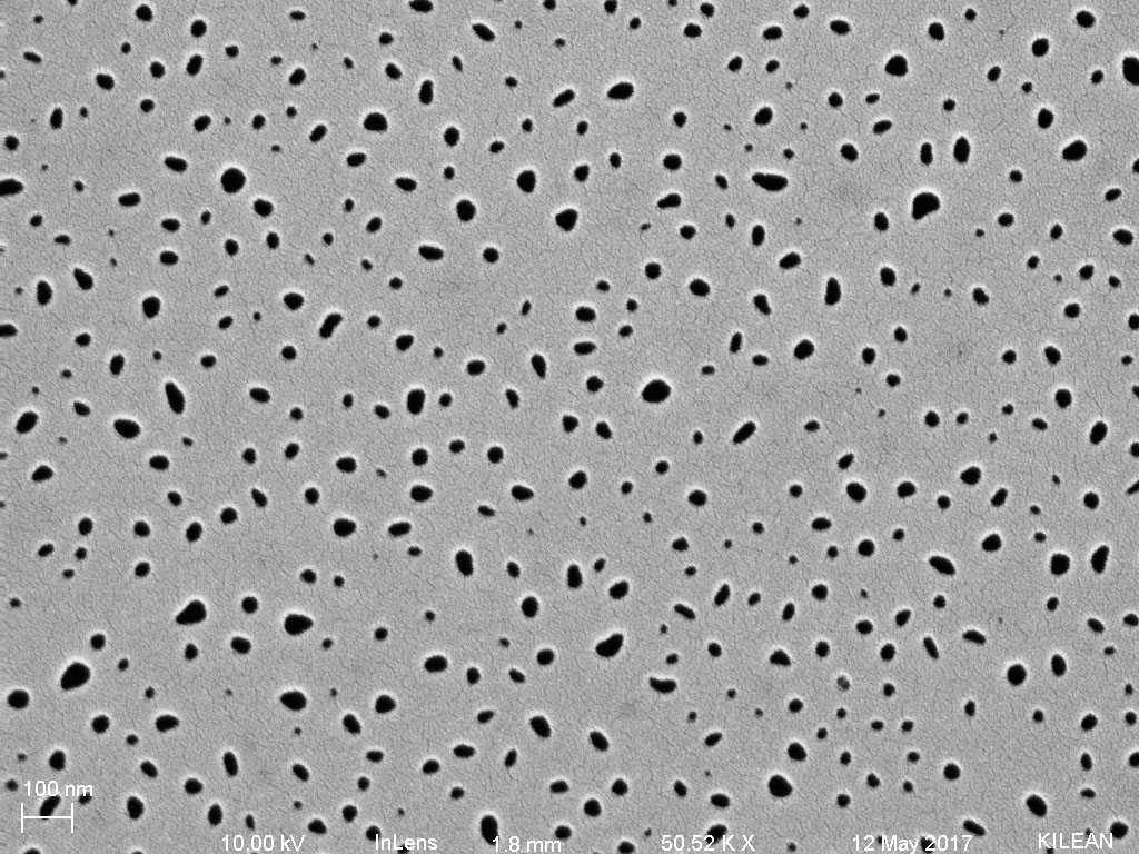
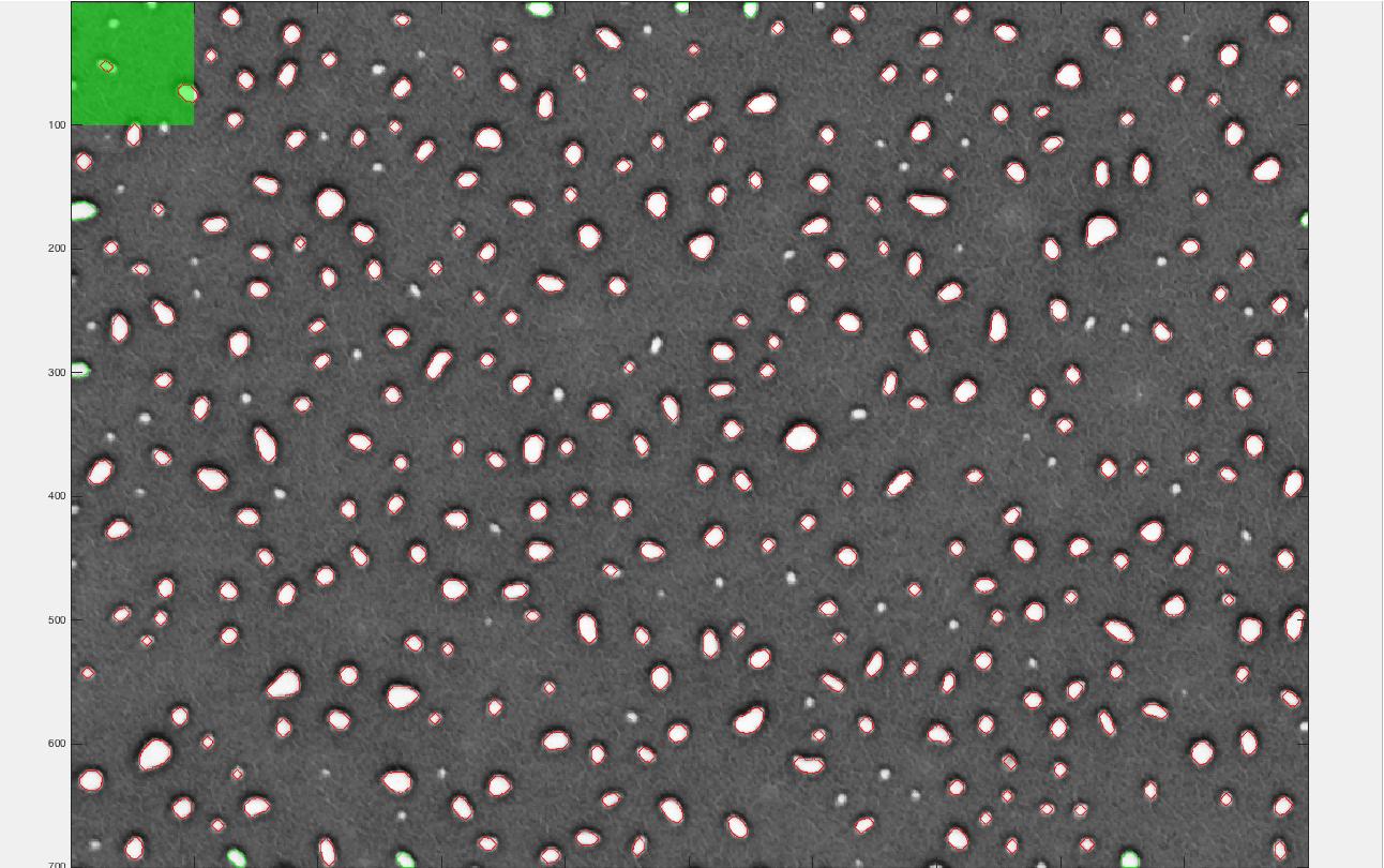
Greg helped me run a pore analysis. These are those preliminary results. I will run more images and see if these values hold up.

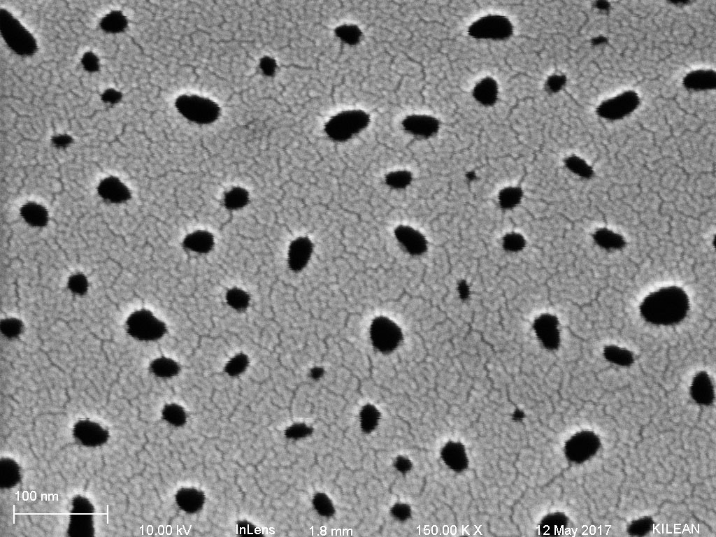
Much prettier on the backside. Did you get an average pore size?
I’m still working on getting more accurate results from MATLAB. The example in this posts ignores many small pores. The smallest, which would usually be considered pits if see on the top are actually through holes as they appear on the bottom. I’ll get better and more thorough results soon.