Post-etch annealed membranes
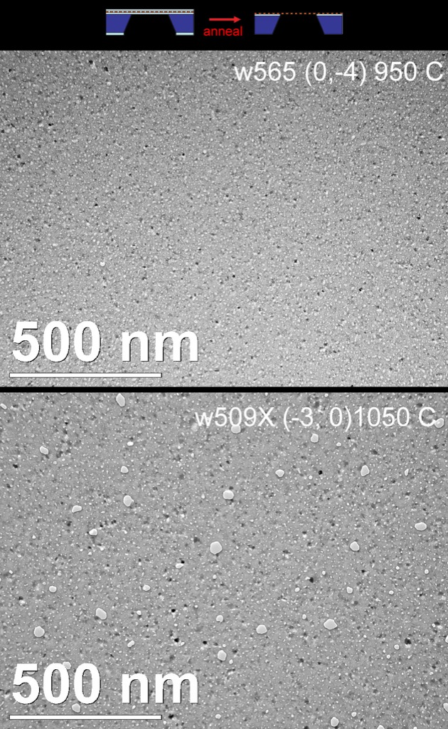
Below are images from two samples that were annealed at 950 C and 1050 C post-EDP etch. The lower temp anneal produced a membrane with many features that do not seem to penetrate the nc-Si. There were a few (couple in each field) smaller pores ~ 10 nm in the outer samples. This supports Jess and Karl’s dye diffusion and air permeability story.
The high temp anneal generated pores that are 40-50 nm in diameter. The next step will be to tune annealing temp and study how porosity & cutoff change.
The full set of images can be found on the NRG photos site.
The largest pore I see has a diameter of ~42nm, so this is the highest cutoff I would expect. I also get a porosity of ~2.5% if you include the brightest tiny pores, 1%-1.5% with just the large pores.
It is interesting that we see non-uniformities, as the wafer is no longer playing a role. This is useful info, as we try to explain the observed differences between thermal and TEOS processes.
Interestingly, these results absolutely confirm that the pores are formed during the annealing process, so Philippe can stop worrying about it.