200nm thick Si film from the NSN stack
During my visit last, I deposited a couple of wafers and one of them is to test a even thicker Si film from the NSN stack. The thickness for the Si film is 200nm and the nitride layers are still 30nm. After deposition, the Si wafer was etched and the pop-out TEM grids were then annealed at 1000C for 1 minute with a 50C/s ramp up rate. The following are the TEM images of annealed samples.

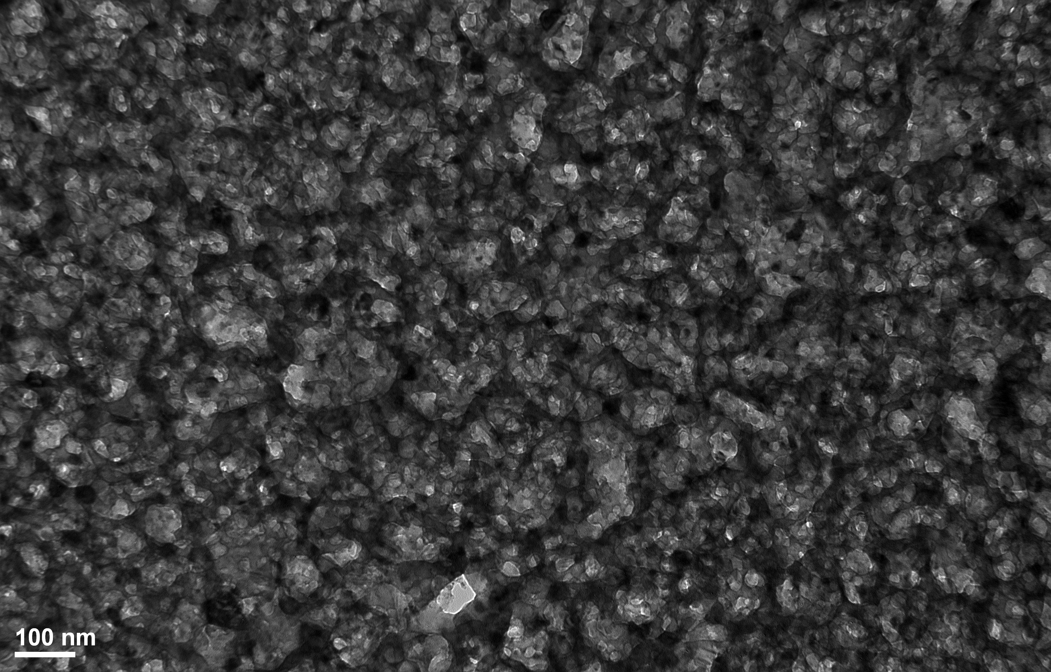
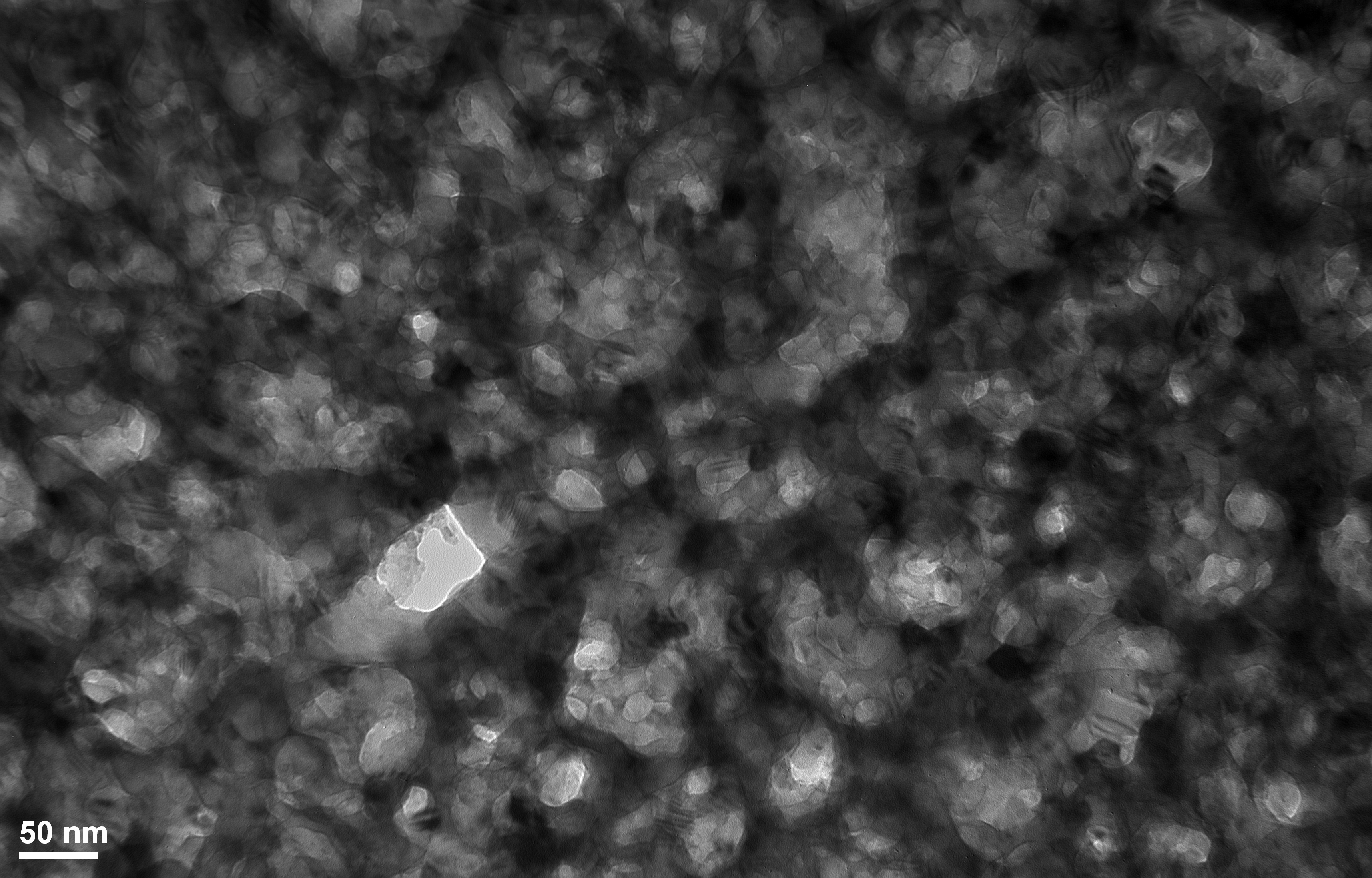
As it can be seen from the above TEM images, very few through pores can be formed in the 200nm thick silicon film after annealing, which is not surprising since the silicon film is quite thick. However, “pits” features are all over the silicon film. It indicates that these pits which were formed during annealing process are not able to go deeper through the silicon film to form pores. This experiment shows that there clearly is an upper limited for the thickness of silicon film that through nanopores can be formed.