Thick SiO2 Depositions on Microporous Nitride Creates Infilled Pores
Alec and Elysia’s study on the migration of infectious bugs through microporous silicon nitride has been useful, however, the size range of the pores is not sufficient to halt the migration. To create smaller pore sizes, I infilled the chips from Wafer 4695 (600 nm pores) with SiO2 depositions.
Deposition Settings
- 350 C
- Aluminum Holder (Multiples of individual chips)
- Platen Rotation
- SiO2 (Kurt Lesker)
- e-beam evaporation, 10-14 mA beam current
- 0.7-0.8 nm/sec on average (peaked at 1.2 nm/sec)
- Deposition Thicknesses
- 25 nm
- 300 nm
- 450 nm
- 600 nm
- 800 nm
Native Pore Structures
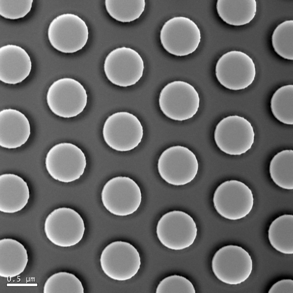
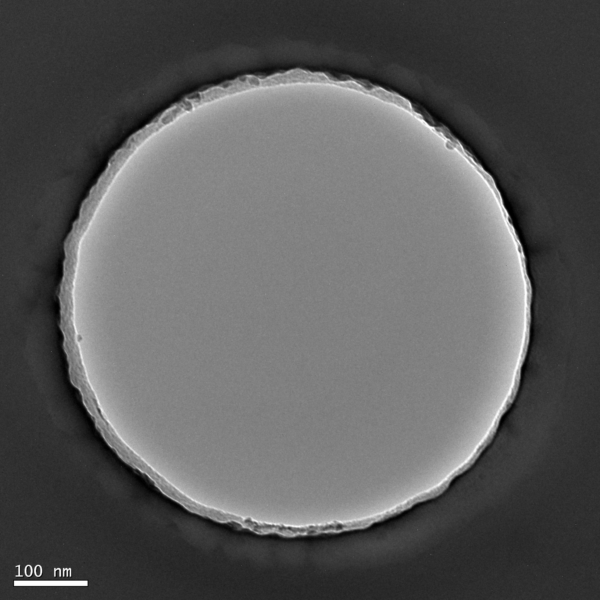
Infilled Pore Structures
+25 nm SiO2
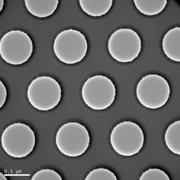
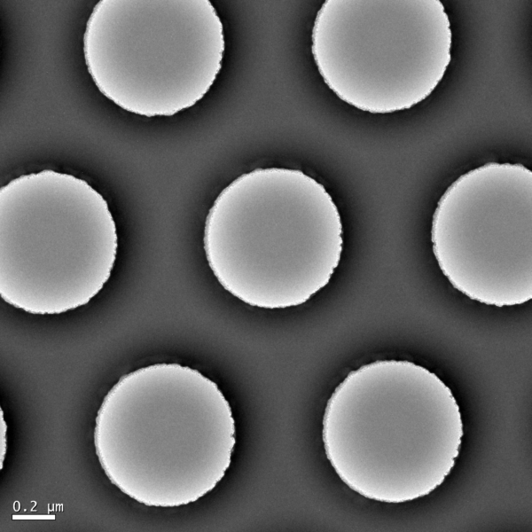
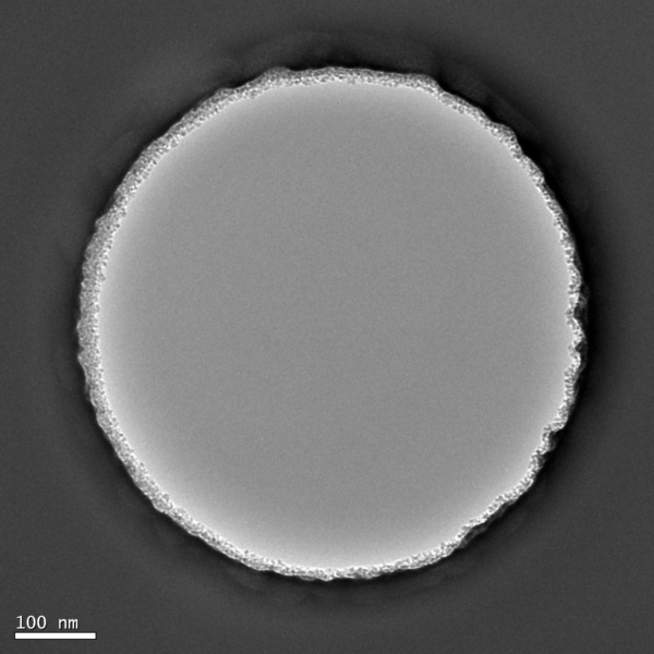
+ 300 nm SiO2
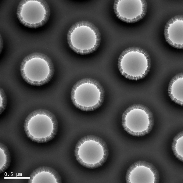
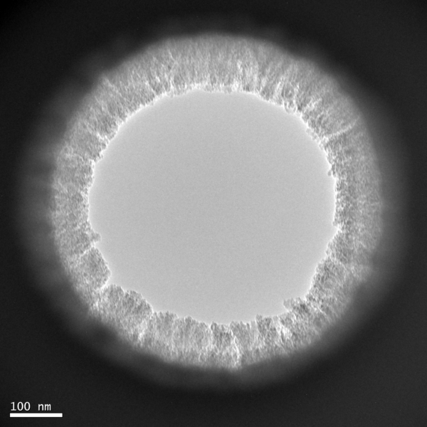
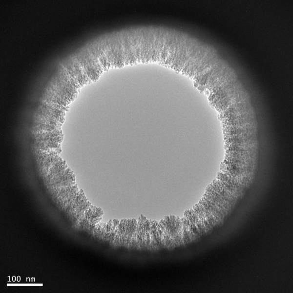
Run 2
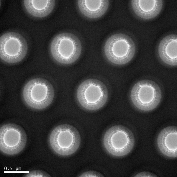
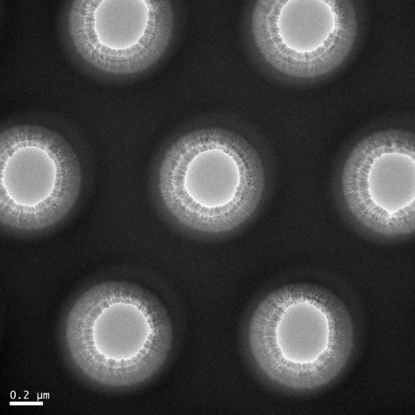
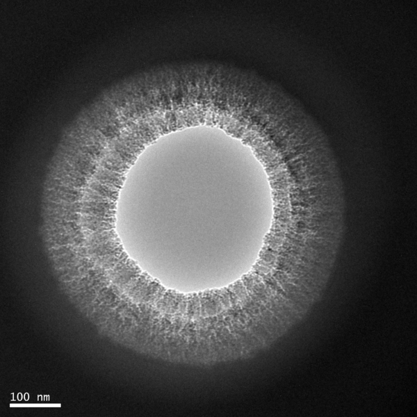
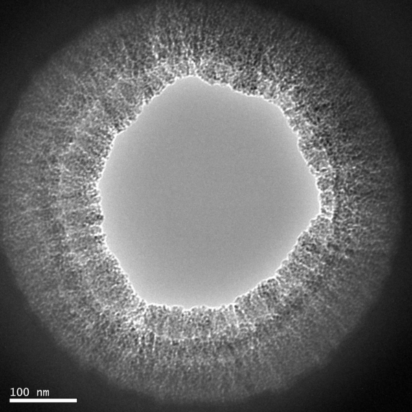
+450 nm SiO2
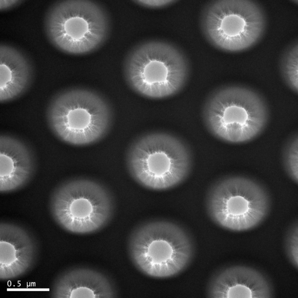
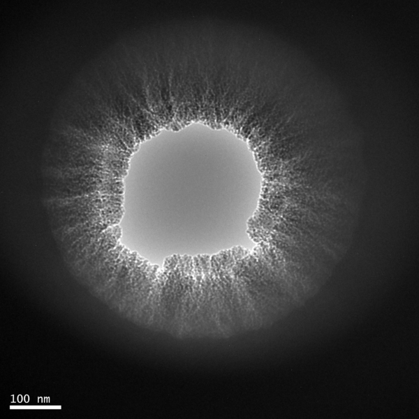
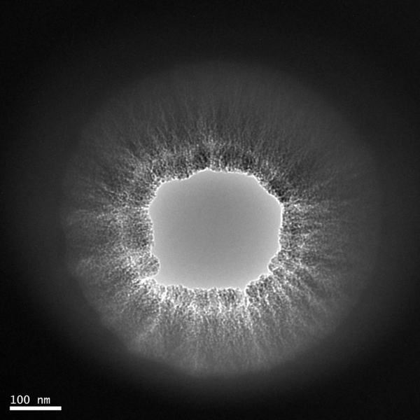
+600 nm SiO2
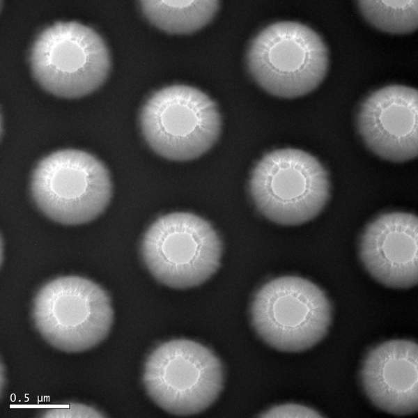
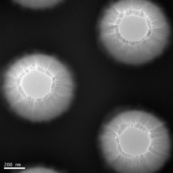
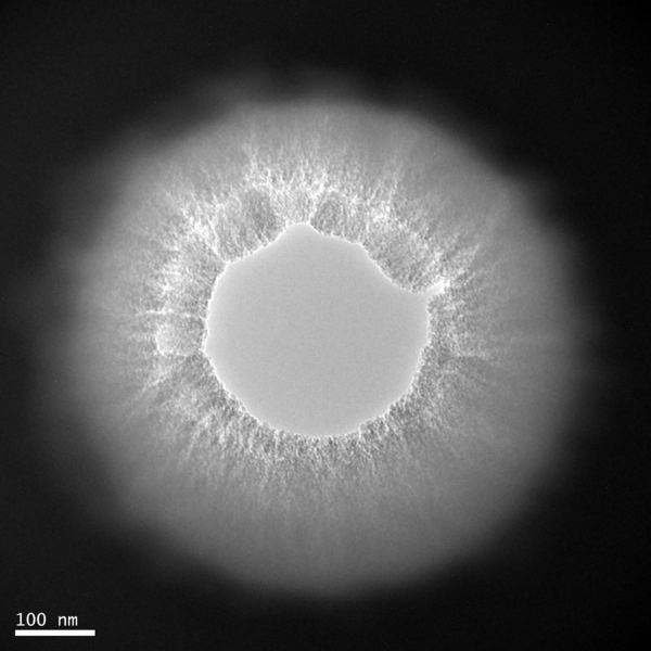
+800 nm SiO2
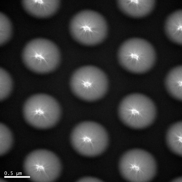
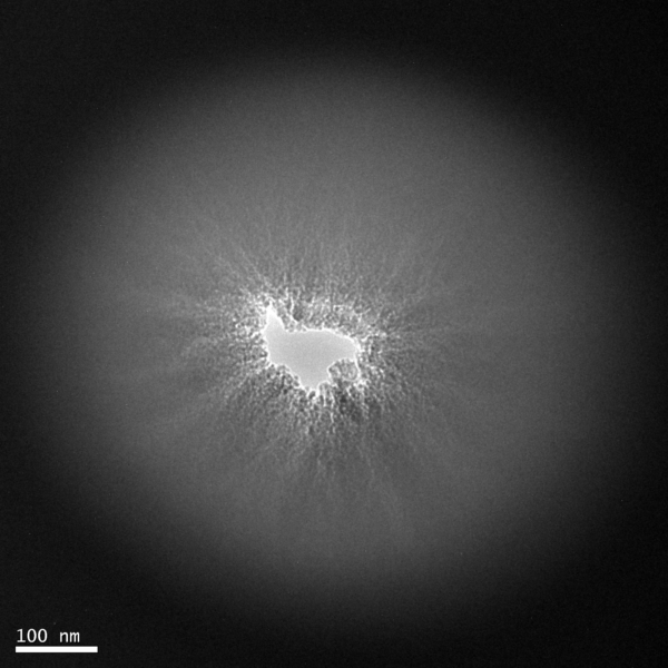
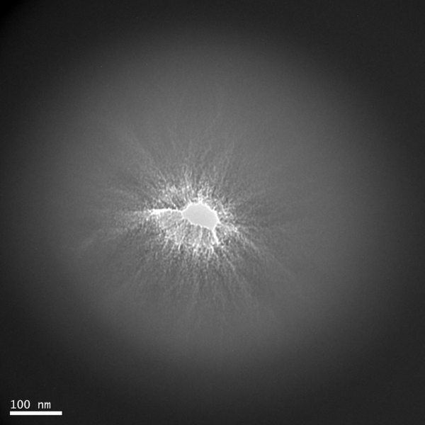
The thicker coatings tend to stress out the membranes, leading to a wrinkled appearance, though they’re all still intact. I would like to see the a few of the chips after the transmigration experiments to see if the pore wall coatings are stable, hopefully not delaminating under wetting conditions.