Production from 1.17.2008
Last week’s production yielded six wafers, all deposited at room temperature. Here were the annealing conditions:
Wafer 334, 343 – RTP @ 975C
Wafer 341, 344 – RTP @ 975C + FA @ 1000C
Wafer 342, 345 – FA @ 1000 C
Pinhole density was moderate along the edges of the wafer, with one or two pinholes in ~ 50% of the outside samples. Copper also continues to be a problem as evident in the EDX spectra and TEM micrographs.
Wafer 334 (0,0)
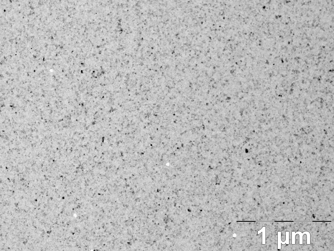 Wafer 334 (0,-5)
Wafer 341 (0,0)
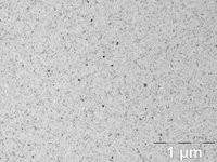 Wafer 341 (0,-5)
 Wafer 345 (0,0)
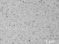 Wafer 345 (-5, 0)
 Wafer 341 (0,-5)
 Wafer 345 (0,0)
 Wafer 345 (-5, 0)
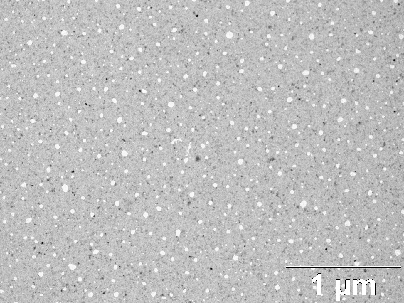 Cu (?) tear in wafer 341
 The tears seem to be more prevalent in samples that saw the furnace anneal. The RTP-only wafers (334, 343) have fewer tears compared the to the FAed wafers. In fact, wafer 343 had no trace of Cu according to EDX, but 334 did… so it’s all still a mystery.
A full set of images at different mags. is in the TEM directory.
It’s interesting that 344 and 341 look so similar, while 345 has much larger pores. If we could just make them smaller, get rid of the copper, and improve uniformity…