Macro To Represent Wafer Characterization
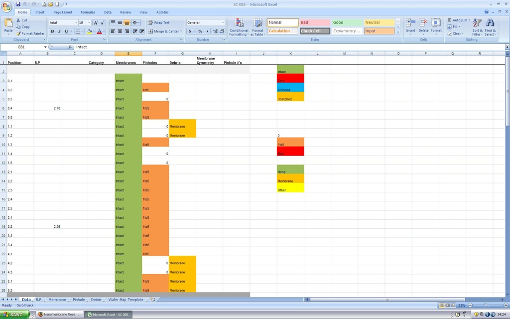
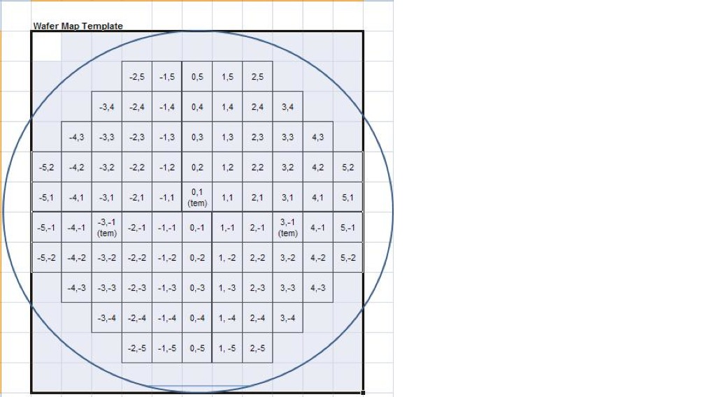
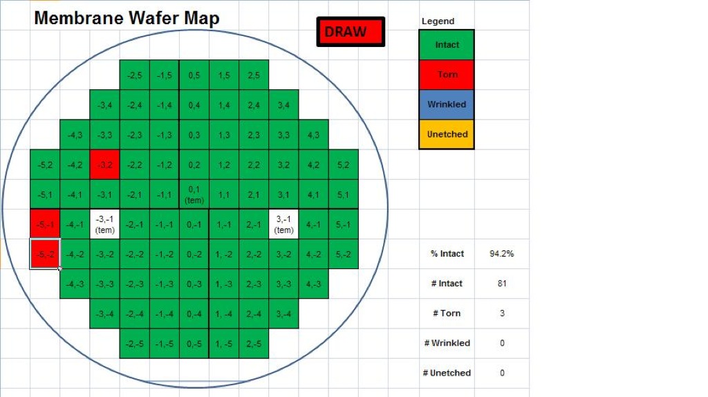
Charles designed a macro for excel to represent the data gathered from wafer characterization, in a visual format. It is built on VB platform and runs off Microsoft excel. The data is input in a simple fashion by selecting the relevant field from a drop down box for columns representing different positions (see fig. 1). This is very similar to the format I used to collect data on Google documents. The advantage is that sep-con format users will be able to take a quick glance at the images to identify the defects on a wafer and to see how many intact usable samples are present on a wafer. One can also deduce whether different quadrants seem to behave differently.
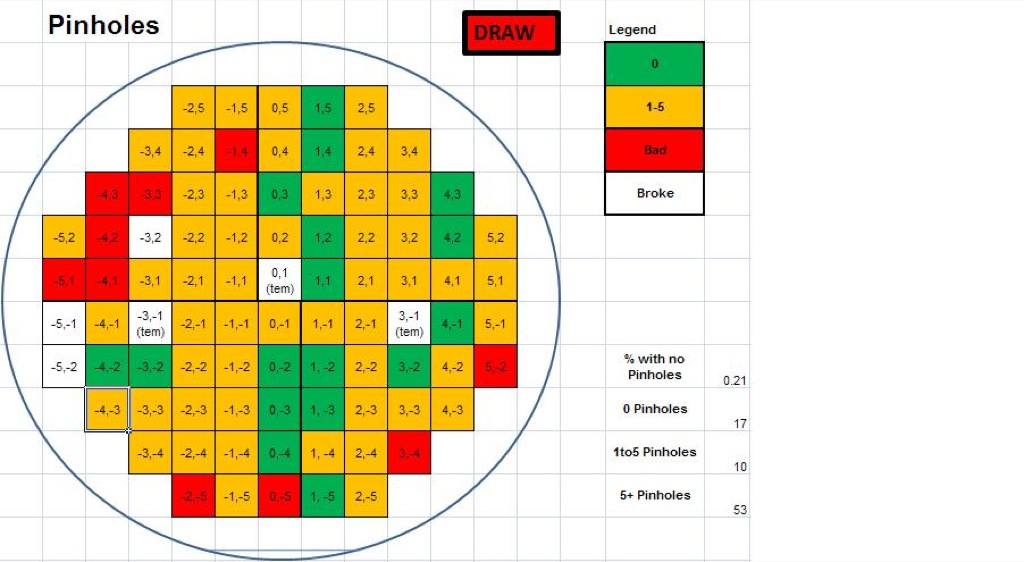
Specific features to keep track of:
-The pinhole number is not visible on the image. It has been characterized into 3 ranges. 0-having no pinholes. 1-5 pinholes per chip. > 5 pinholes- Bad
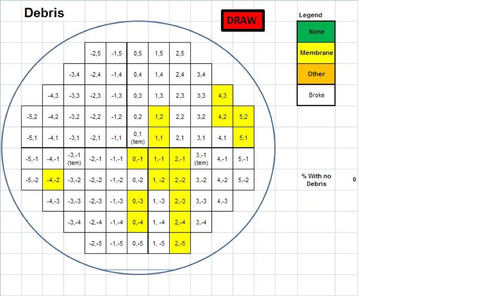
– Debris image will show debris across the wafer and whether it lies over the active area or not.
-Membrane image shows how many intact chips are present on a wafer and their location. It will also show when a membrane has wrinkles or is under-etched.
– Along with these images, a legend shows the % ‘s associated with each image such as % of overall intact samples etc.
The master document for each wafer with the actual number of pinhole for each single wafer will still be on google documents if there is a need to access the information.
I really really like these wafer maps. They answer nearly all the standard questions that I have. Many thanks to Charles for developing them, and Nakul for helping with the interfacing to your data!!
The only question that comes to mind involves the type of debris. I’m not sure if it requires it’s own map, but how can I figure out what type of debris it is and when it got there. Fresh from the cleanroom, the most common debris will probably be membrane pieces, occasional particles, and chemical residues. After punching them out, the common debris will be shards of wafer and membrane pieces from the outer edge. We need to have some way to sound the alarm if any of these get out of control and an understanding of which one causes the most fallout. Any ideas?
I was interested in the debris map only because sometime people might be hesitant using samples with debris sitting on it as it might affect experiments. Otherwise when i inspect the wafer, I keep a look out about what kind of debris it is, since it is relatively easy to identify the source of the debris.