Burst Pressure Vs Thickness Series( 50 nm vs 30nm)
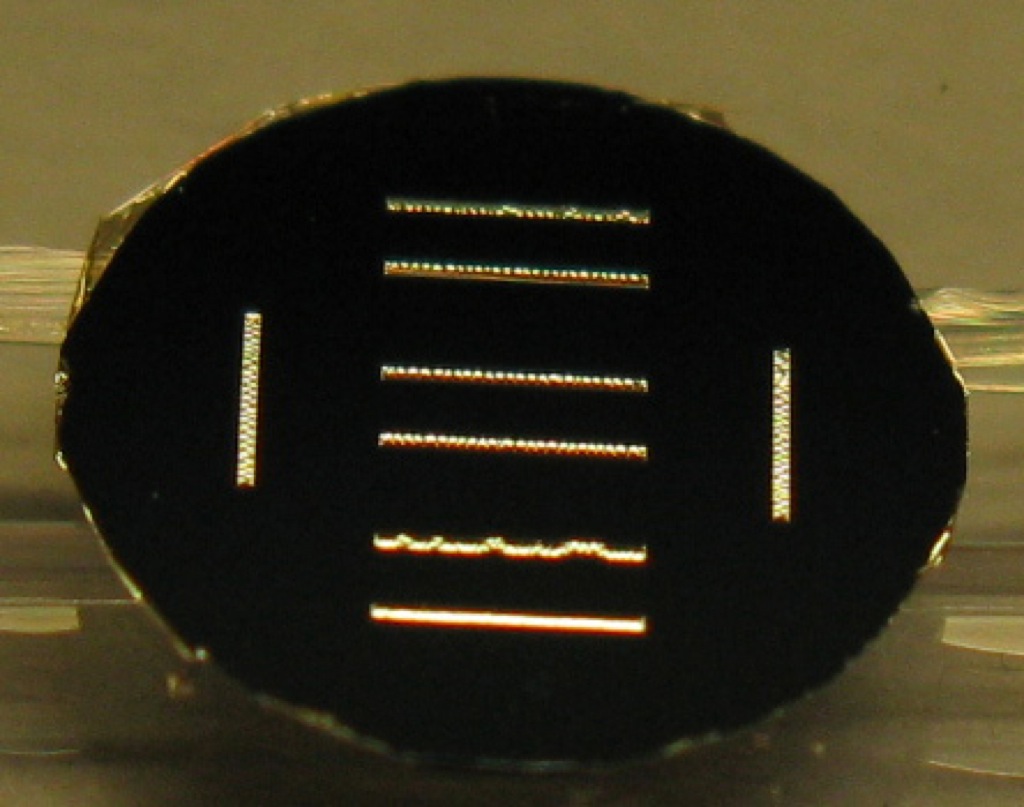
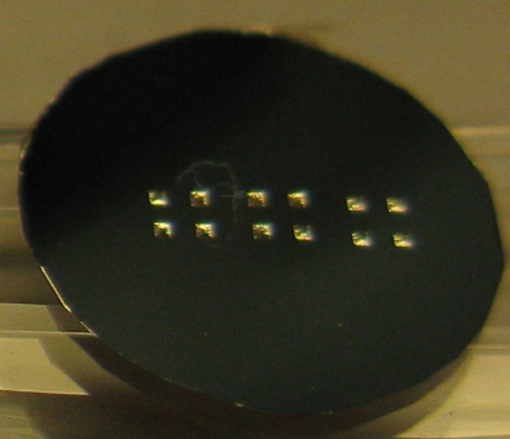
Last week Dave deposited sep-cons ( cell culture mask) with 3 different thickness namely the regular 15nm , 30 nm and 50nm ( SC 142, 143,144). These wafers were characterized and it was noted that the 15 nm had a high pinhole density and the 30 and 50 nm films were low pinhole density. The cell culture masks were circular sep-con pattern wafers but had different active areas on each of the chips. They were 2,4,6,8 slots or 12 squares.
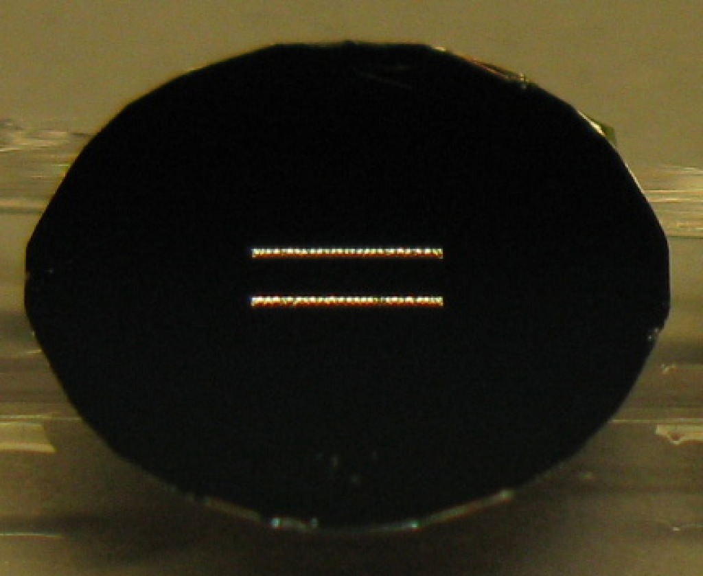
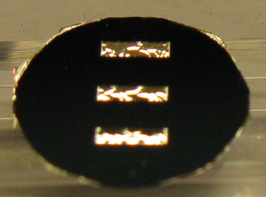
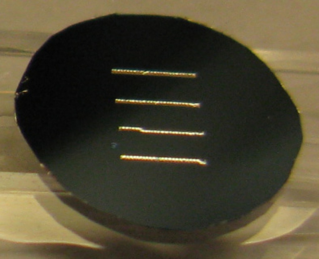

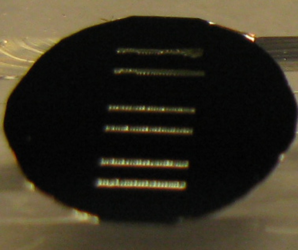
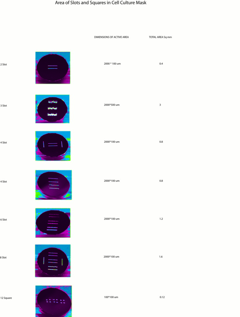
ACTIVE AREA DIMENSIONS
Burst Pressure tests were performed for a a variety of samples from the 30 nm and 50 nm films. The samples tested were pinhole free and from the same position (across the 2 wafers) for comparision.
The 50 nm thick 2 slot films were noteworthy as all tested samples were above 15p.s.i and the highest recorded was 21.7 p.s.i.


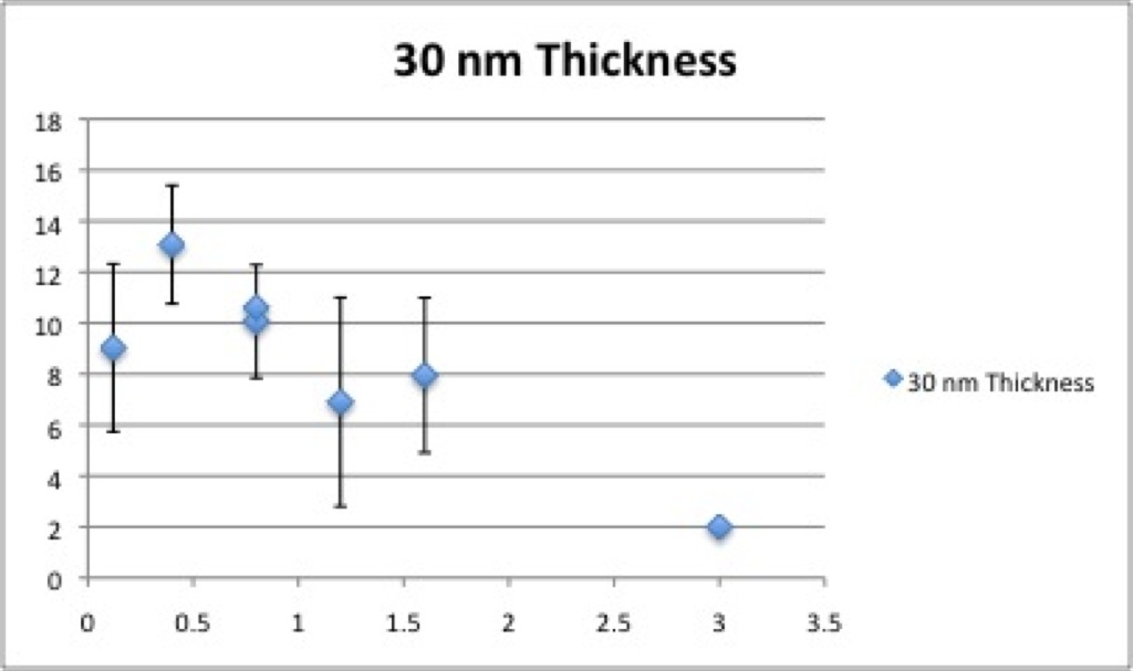
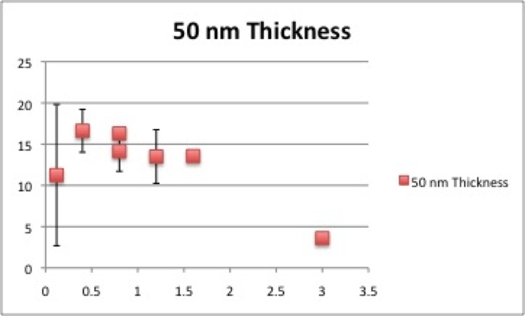
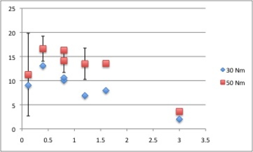
The 3 slot had the largest active area and was also the weakest in both cases. The 2 slot was the strongest pattern. Apart from the 2 slot pattern, all samples had a larger surface area than regular sep-cons.
The wafers appeared to be dirtier than regular which could explain the high pinhole density in the 15 nm sample. This may also have lowered our burst pressures.
Attempted 3 D plots Comparing active area vs position vs BP for 30 nm Films
(Note: All pictures are the same in different orientation)


Thanks Nakul. There is a lot of information here, but we still need a little more.
The images you show with slits have all the same slit size. The 3 slit arrangement is not shown, but these were wider slits, correct?
Can you make a table listing the chips by name, the total active area and the dimensions of the individual membranes on these chips?
What are the appropriate units for the x-axis in the Area vs. BP plot? I’m guessing the ‘3’ is the large format three slit geometry. I don’t know where the 12 squares reside.
We worry about shape and total active area affecting overall stability. I think there is enough data here to help in the design of a dedicated study.
The improvement with thickness gives us reason to be optimistic.
When I made this mask, I basically cut and pasted shapes from the standard TEM and 2-slit Sepcon patterns.
Assuming that the etch was “typical”, each square should be ~ 100 microns x 100 microns. Each slit pattern is a multiple of the single 2000um x 100um slit area. The large slits are each 2000 um long and should be ~ 200 microns wide, although they look a bit wider (by eye). I guess they should be measured with a micrometer to be sure.
In the area vs bp graphs, the x axis refers to the active area per chip. The 12 squares are the first point on the graph, as they have the lowest active area. The 3 slot shown in the pictures has an area of 2000*~500 um.
There is really no logical reason why the thicker Si films should have lower pinhole density, and I don’t think this trend has been seen before. Does anyone on the production side have other information about the etch or the cleanliness of the 15 nm sample that could shed some light on this?
Either way, this should be repeated, probably next week?
We also need to have a discussion about active membrane area on our SepCon samples for experiments. We seem to be making considerable progress in lowering pinhole density, so it may be an appropriate time to play with some other patterns that offer larger areas and migrate away from the current 2 slot pattern. I would suggest widening the slots and adding a few more, but I’m open to suggestions. We also have the (110) wafers to try.