YES System / Silane Vapor Deposition system – Initial Trials
All the data presented below was generated by Alex from Adarza Biosystems, Inc.
Introduction:
Chemical vapor deposition of 99% APTES (3-Aminopropyltriethoxysilane) on planar silicon chips was accomplished using the new vapor deposition system (YES: Yield Engineering Systems). In addition to vapor deposition of chemical moieties, YES system is also equipped with plasma cleaner that enables cleaning of substrates with oxygen plasma.
Oxygen plasma: Oxygen plasma in the YES system is generated by the oxygen present in the chamber @ pressure of 0.5 torr and in the presence of ~ 198 KW of energy. Oxygen plasma comprises of high energy ions, oxygen radical and electrons. Oxygen radicals attack the hydrocarbons on the surface of the substrate and oxidize them and hence render the surface free of organic residues. Oxygen plasma is generated between two electrodes in the chamber know as the active shelf and the ground shelf by the energy applied in the form of radio frequency. Right below the ground shelf in the chamber is the floating shelf on which the substrates to the treated are placed. This configuration of the shelves/plates in the chamber will be called as the downstream float configuration for our future reference. This in general is the preferred configuration of the shelves as the presence of ground shelf right above the floating shelf absorbs all the high energy electrons which can otherwise damage the sensitive substrates on the floating shelf.
Procedure of silanization: The chips were initially subjected to 5 mins of oxygen plasma treatment following which the chips were hydrated in order to generate reactive hydroxyl groups on silicon dioxide surface. Following this, the chips were subjected to the vapors of APTES for 10 mins. At the end of which the chamber was purged in order to vent out the excess silane vapor. Note: The chips before placing inside the chamber were pre-treated with base wash (7:3 of 10 M NaOH to ethanol) for 30 mins with mild shaking. One set of chips were then placed inside the chamber post base wash and the other set was subjected to 30 mins of piranha ( 3:1 of con. H2S04 to 30% H2O2) wash under mild shaking conditions.
Results: Tabulated below are the spectroscopic ellipsometry measurements of the APTES layer in Ångstroms) on planar silicon chips post vapor phase silanization carried out in the YES system.
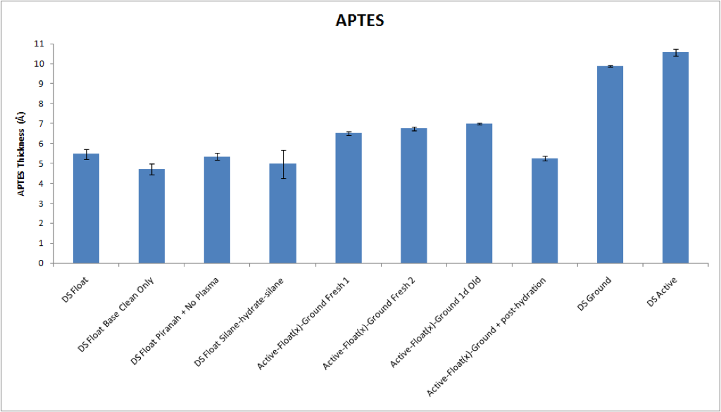
Note:
DS Float – Silicon planar chips were base washed then piranha cleaned following which they were placed on the floating shelf which is downstream (DS) of the ground shelf.
DS Float Base Clean only– Here the chips were only subjected to base wash after which they were placed inside the chamber in the same configuration as above.
DS Float Piranha– Here the chips were piranha cleaned and then placed in the inside the chamber in the same above configuration. Once inside the chamber the chips were not subjected to plasma treatment instead were directly exposed to APTES vapors.
DS Float Silane-Hydrate-Silane– Here the pre-treatment of the chips is as in case of DS Float. After the first silanization process the chips were once again hydrated and then subjected to vapors of APTES for the second time.
Active-Float(x)-Ground Fresh 1 – Here the pre-treatment of the chips is as in case of DS Float. Chips in here were placed on the floating shelf which was now in-between active and the ground.
Active-Float(x)-Ground Fresh 2– Trial 2 of the above done on a different day.
Active-Float(x)-Ground 1d Old- Here the chips treated with base wash and piranha were left @ RT for 1 day before subjecting to APTES vapors.
Active-Float(x)-Ground- post hydration– Same as Active-Float(x)-Ground Fresh 1 but for the post hydration step after the silanization.
DS Ground– Here the pretreated chips (base washed and piranha cleaned) were placed on the ground shelf instead of floating shelf.
DS Active– Here the pretreated chips were placed on the active shelf.
Discussion: Looking at the results from the first three experiments suggests that when the chips are pre-cleaned and placed on the floating shelf which is below the ground shelf in the chamber, the thickness of the silane is ~ 5.5 Å. When the chips were subjected to second round of hydration after silanization ( to check if the surface is fully hydrated post 1st round of hydration), there wasn’t a significant difference in the thickness of the silane put down. Next when the configuration of the shelves was changed such that the floating shelf is now in-between the active and the ground the thickness of the silane layer significantly increased to ~ 6.5 Å. In order to check if the 1 Å increase in the thickness was due to the more silane deposition or was just some atmospheric residues adsorbing to the surface, the chips post silanization were again hydrated. These chips now measured ~ 5.5 Å for silane suggesting that the increase seen earlier was contributed by some adsorbed moieties and not silane. For the last two set of experiments, thickness of the silane layer is ~ 10 Å. Alex has observed (data not shown) that when the chips are placed directly on the ground or on the active shelf, oxide thickness post plasma increases by ~ 5.5 Å and this shows that net thickness change observed when the chips are either placed on the ground or the active shelf is ~ 5 Å. (Note: Theoretical thickness of the monolayer of APTES is ~ 7.5 Å).
Is there a ref for the theoretical thickness? Is that a calculation based on bond lengths?
Some of the papers I’ve read mention that a thickness of 9A is a good monolayer of silane. Is that because that’s “close enough?”