SiN-NP with varied RIE times
We used 4″ wafers with 40 nm pnc-Si on 50 nm RV SiN (RTP 1050 C, 100 C/s, 60 s).
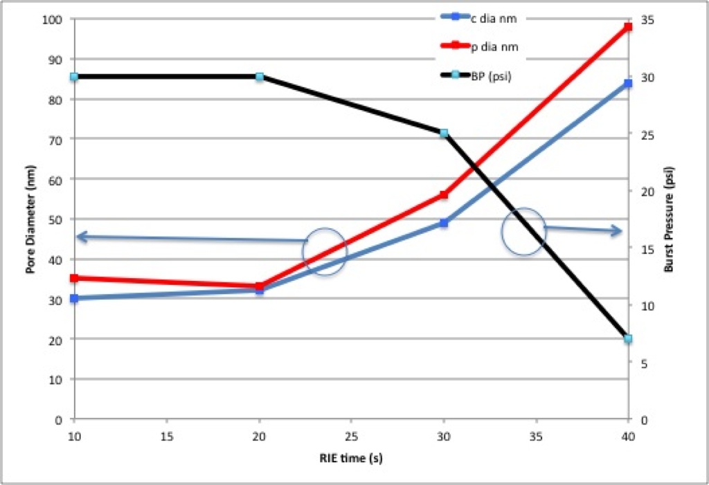
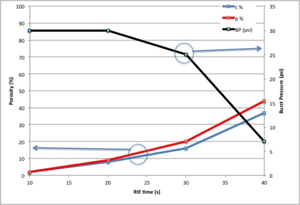
JP ran a series of RIE times from 10 to 50 s with 10 s intervals. (We had initially planned on starting at 70 s based on experiments with 6 ” wafers, but fortunately JP chose to start with 50 s and realized that was already too aggressive. JP suspects the different etch rates are caused by the differences between etching a 4 ” wafer and a 6 ” wafer)
RIE (s) – Wafer #
0 – 1028
10 – 1037
20 – 1036
30 – 1029
40 – 1030
50 – 1031
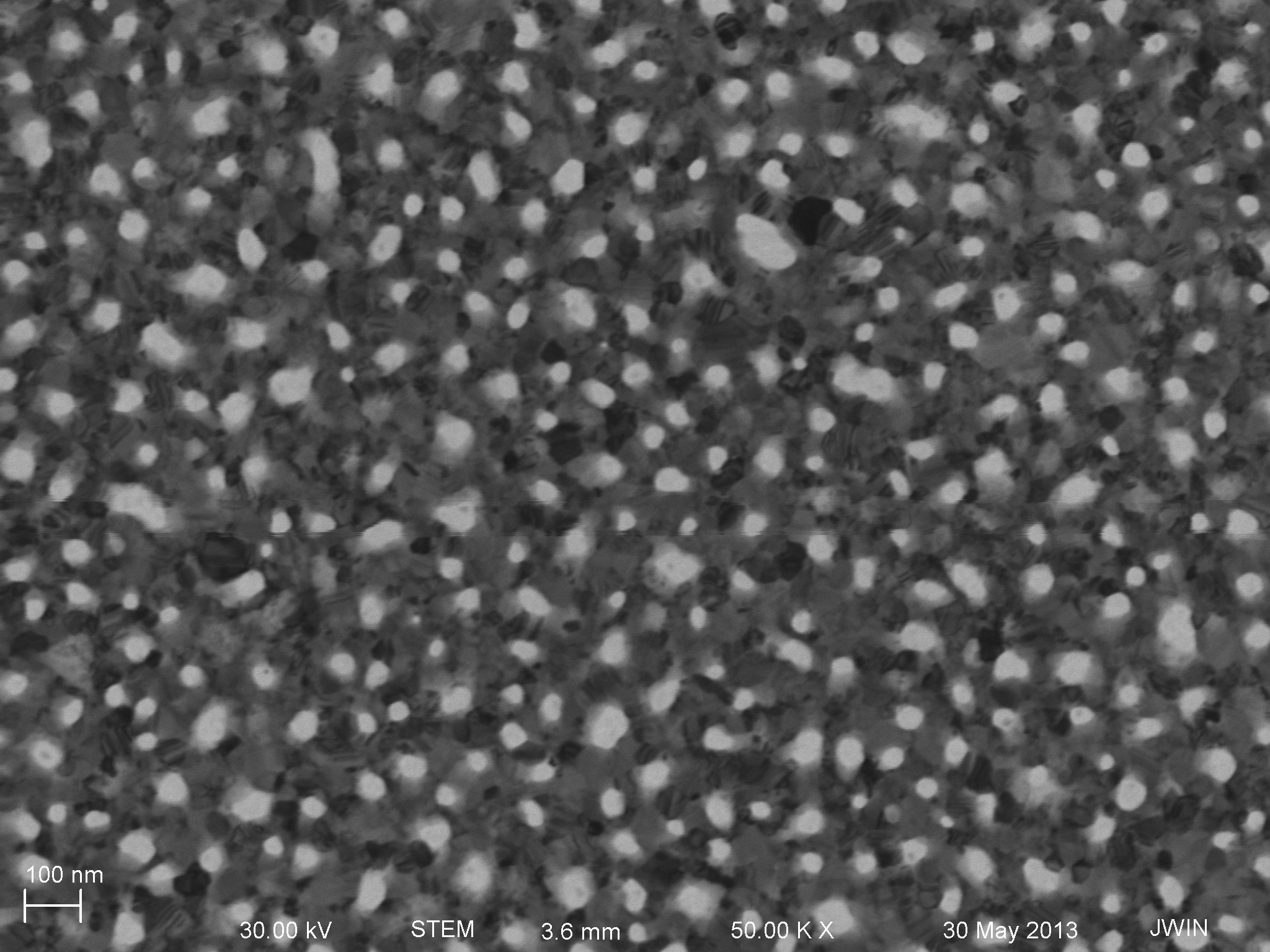
Attached are STEM images used to calculate porosity and pore sizes, which are plotted along with burst pressures. (the max pressure on our tank is 30 psi)
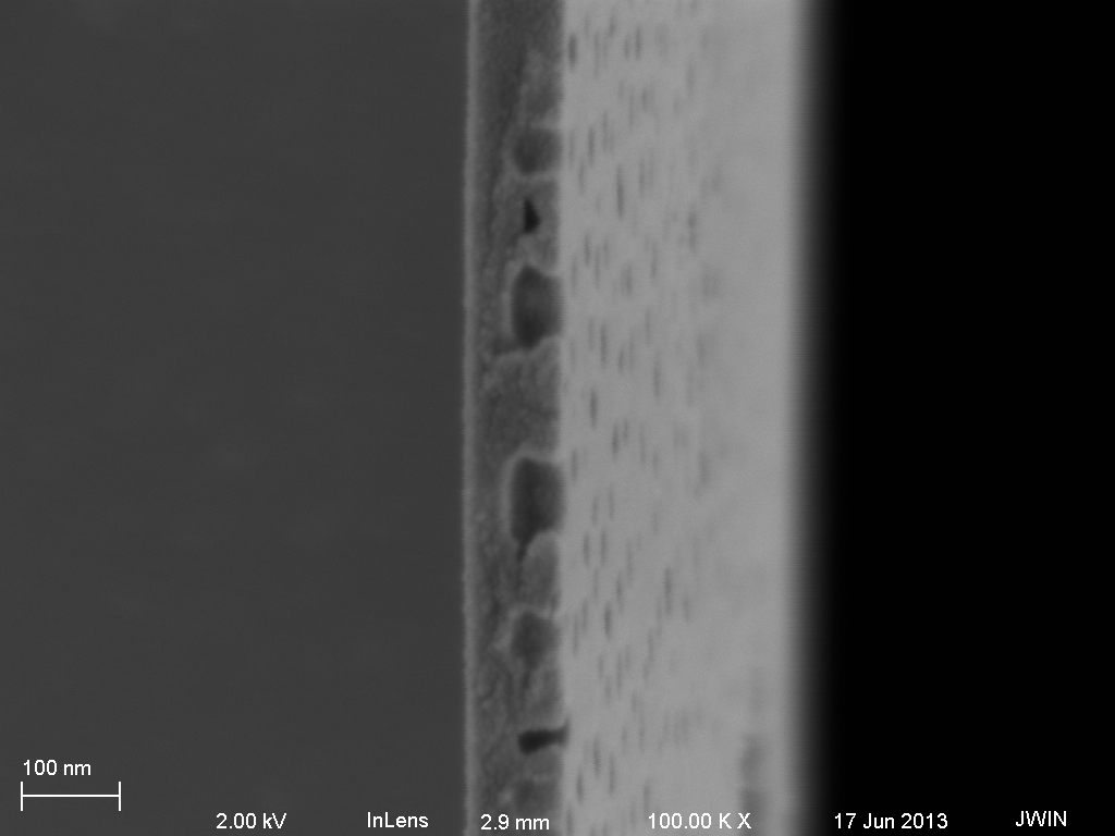
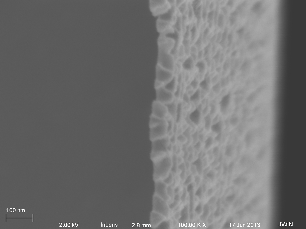
Also attached are SEM images of cross-sections where the Si substrate is always oriented to the left and the pnc-Si layer is always on the right.

- control x-section

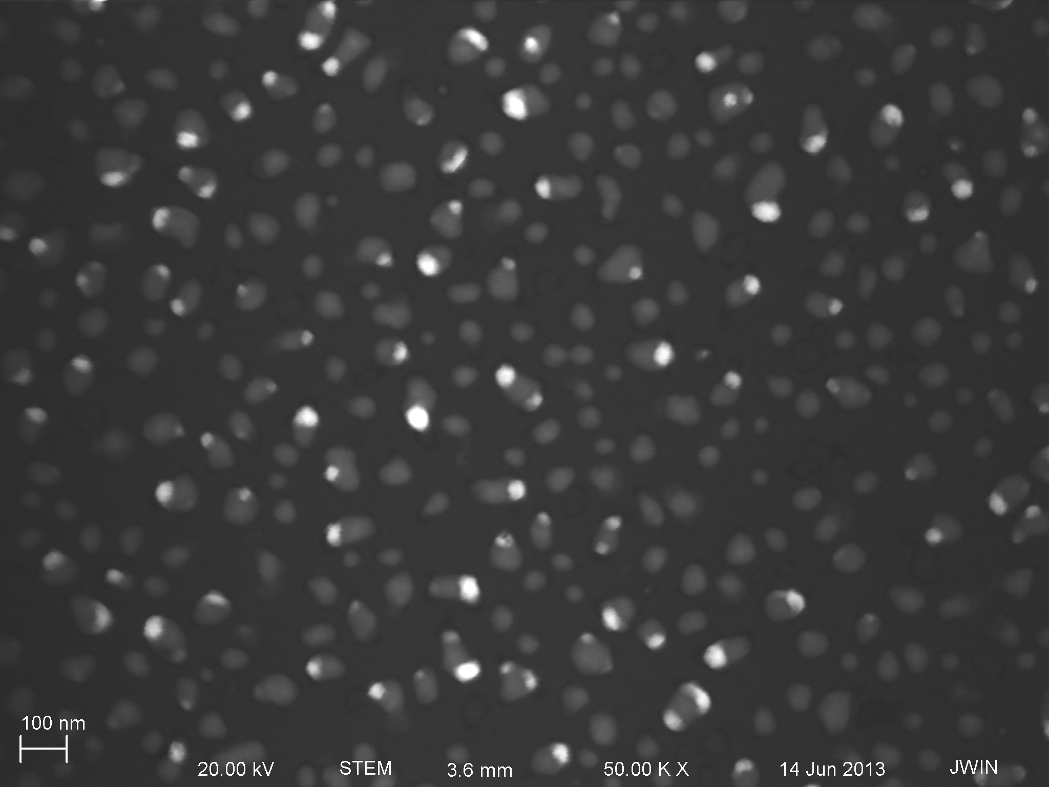
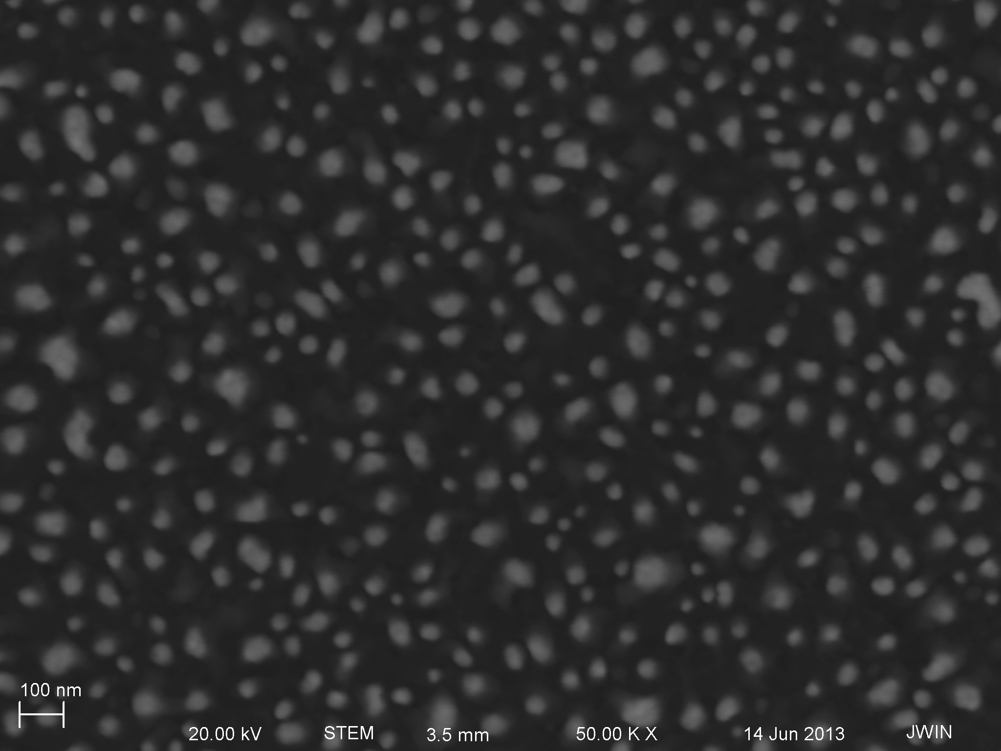
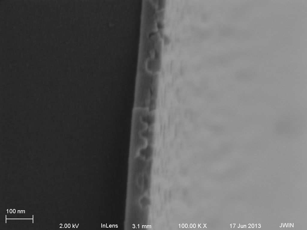
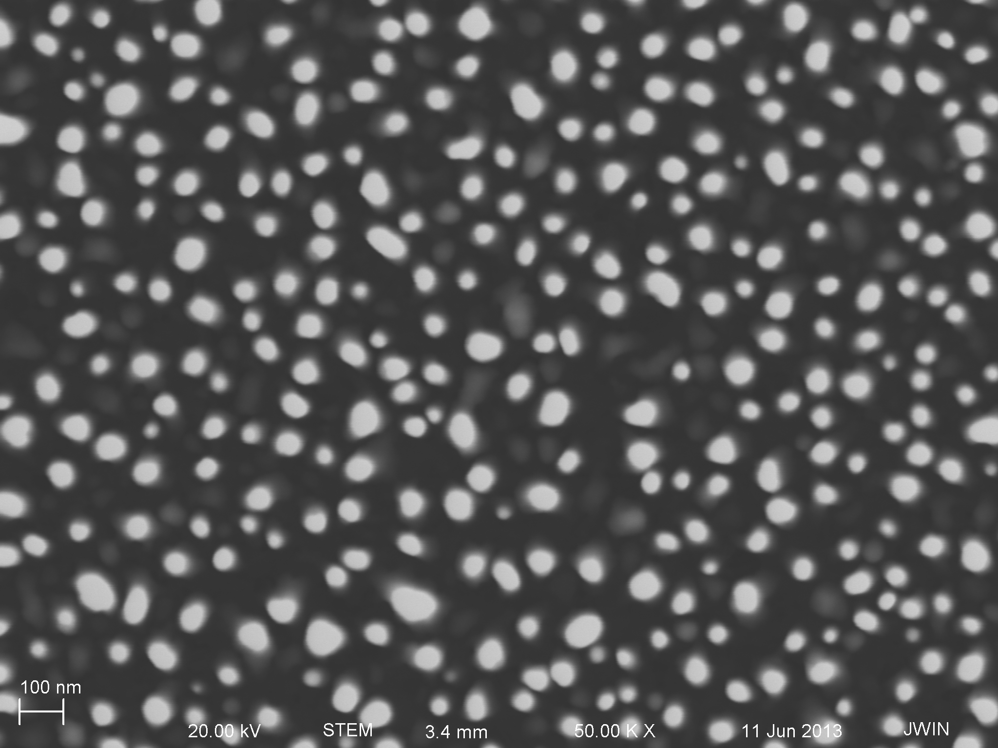
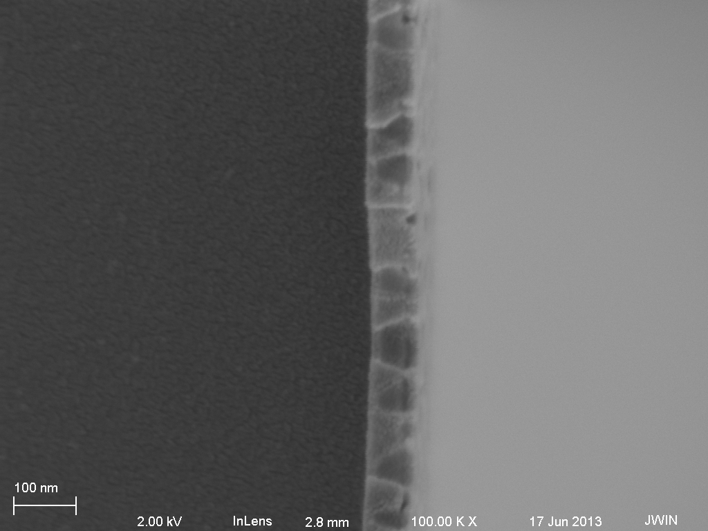
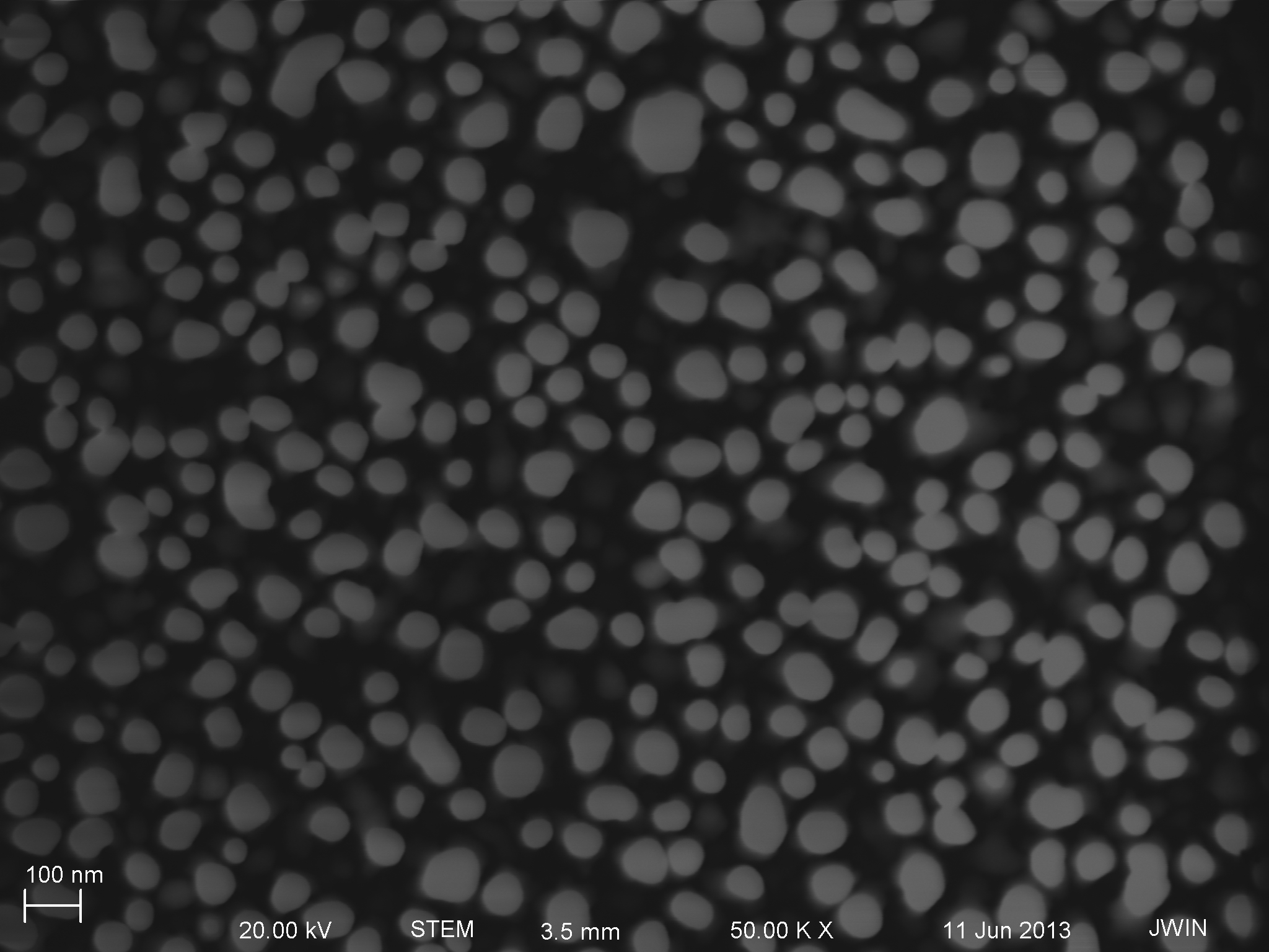
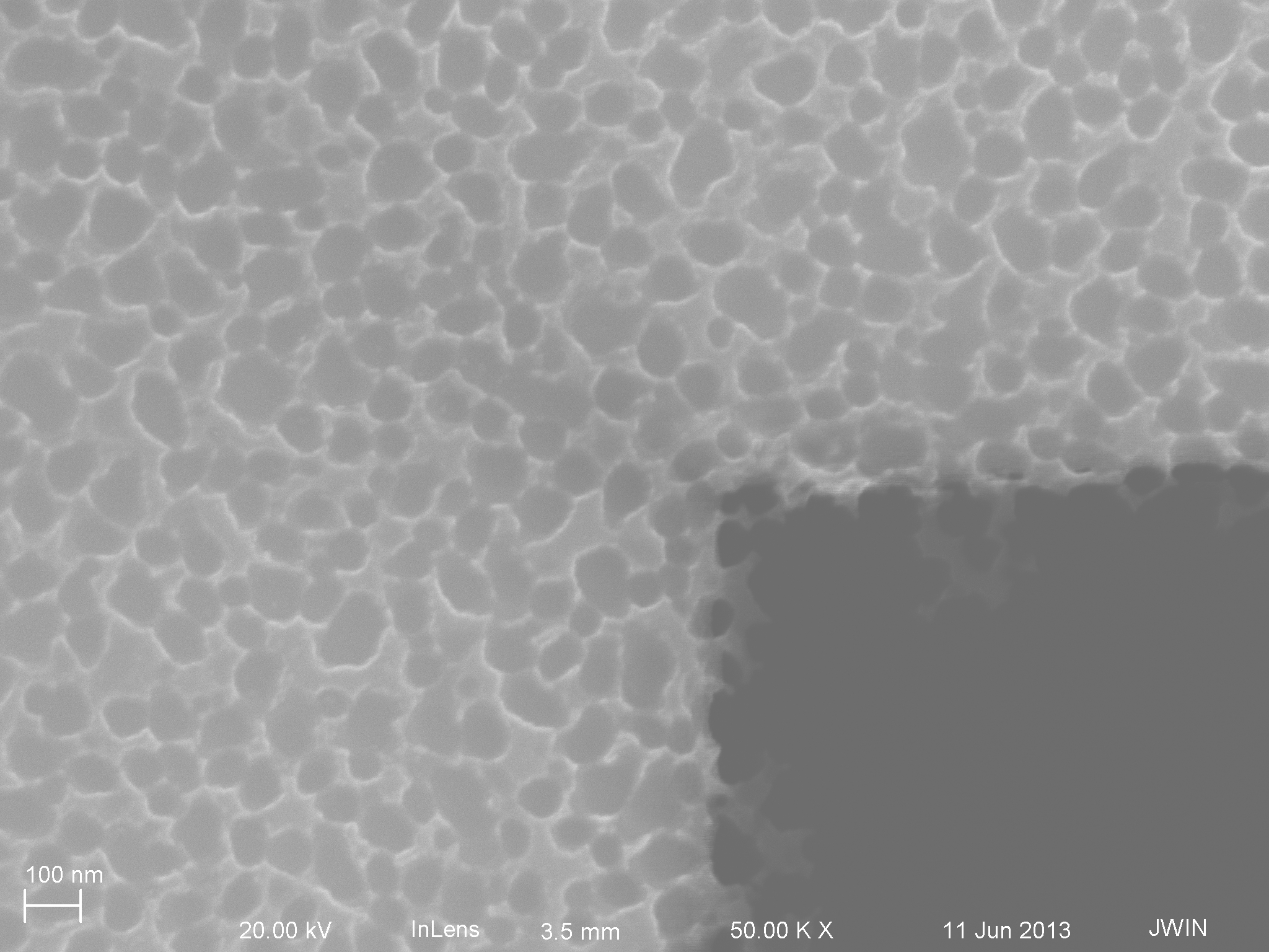
As expected, shorter RIE times lead to lower porosities and vis versa. The control wafer 1028 has a pnc-Si porosity of ~11 % and avg pore dia. ~40 nm. All other porosities are believed to be measured through the pnc-Si and SiN layers. The porosities still need to be verified by permeance and/or hydraulic permeability tests.
Next up, we will attempt some separations of nanoparticles and hopefully some viruses as well.