Magnesium Fluoride Nanoporous Membranes
Wet Etching of Optical Thin Films
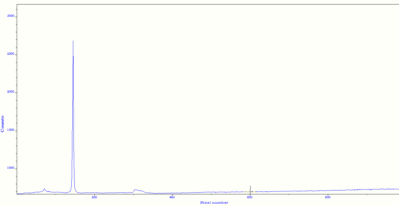
As a result of Christian’s trip and Kevin’s discussions with me, I have been wondering if we could make nanoporous MgF2 membranes for Raman spectroscopy. Part of the appeal in using our Si-based nanomembranes is that the volume they occupy in the observation space is extremely minimal. Even so, a large silicon peak is evident in the background signal.
Christian revealed to us on his visit that he had been able to get a Raman measurement of cells on our native pnc-Si membranes, using 25 mW (TEM grids). The pnc-Si membranes disintegrate at powers much higher than 25 mW. By switching materials, we may be able to make more energetic measurements and improve our S/N ratio.

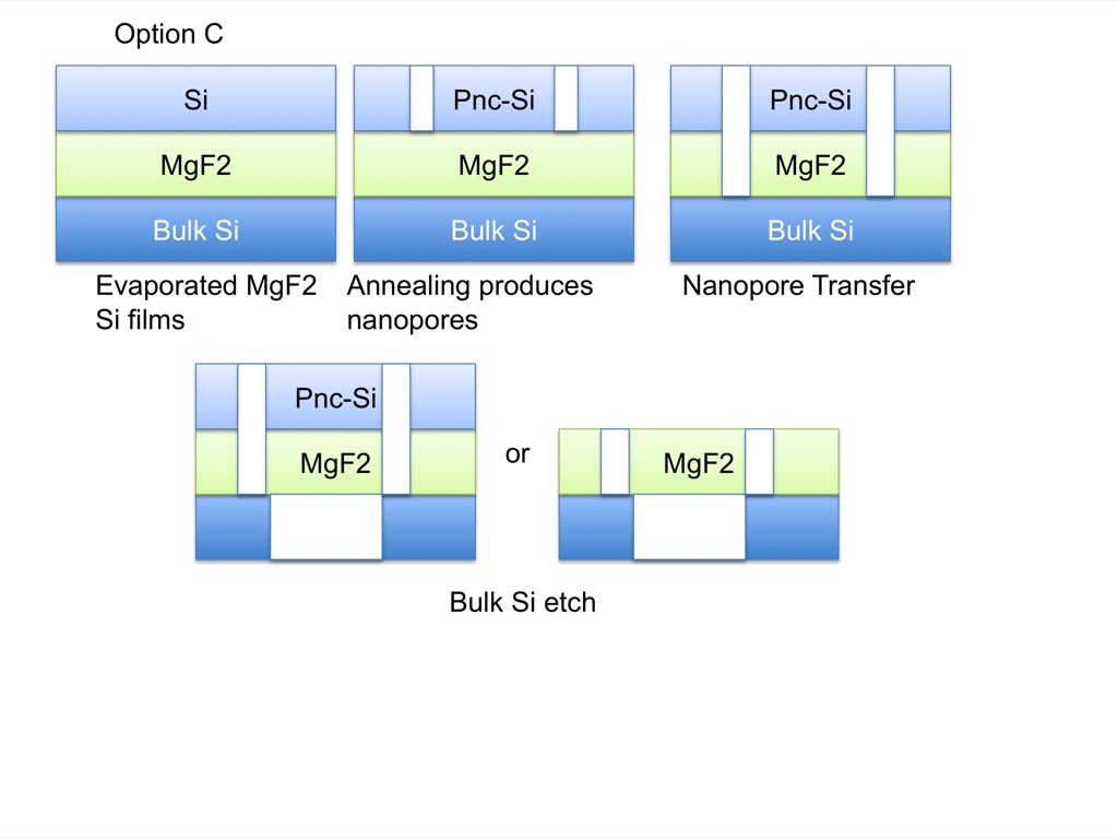
We have potential substrates in Nano-nitride, and pnc-Si materials. Based on the high tensile stress of the MgF2 film in the thesis (evaporated, 300C, 400nm thick, Tensile radius = 50 cm (about 4x less than SiO2)), I would expect that the nano-nitride substrate without the pnc-Si cap would be the best candidate for supporting a free-standing MgF2 nanomembrane. If we have a stable film, the next question becomes whether we can transfer the nanopores into the MgF2 film. In most cases, the thicker film is more stable, but that works against us trying to transfer the pore pattern into the film. Thicker films take longer to etch (need higher etch selectivity) and become more tortured (lower quality transport). Finding a dry etch that has selectivity to support etching a 100nm film is still an outstanding problem I need to solve. If the pattern transfer technique works appropriately, the final process would be to perform a wet etch step to strip the etch mask from the substrate, producing the pure MgF2 free-standing membrane. Luckily, this thesis suggests that MgF2 is particularly inert against many chemical etchants. If we were using nano-nitride substrate, I would use a hot-phosphorous etch to strip the nitride. If we were using pnc-Si, I would use TMAH or KOH to strip the silicon (and use an HF dip to remove the thermal oxide).
![]()
![]()
Alternatively, we could try and make this technique a wafer-level process. The problem as mentioned earlier is that the MgF2 has a high film stress; its not likely to remain an unbroken film through the multi-level deposition and thermal processing. We should begin evaluating this process by seeing if we can deposit and release a MgF2 nanomembrane. The nanoporous pattern transfer can be validated once it is established that we can make a stable membrane.