Anodic Bonding for Flip-chip Microfluidics
Vincent has asked us to integrate our nanoporous filter on top of a thin layer of silicon nitride, so that he can clean up his analyte before being exposed to his single nanopore (fabricated using a dielectric breakdown). There are many different ways to join silicon wafers together. Specifically, we wish to create the following structure:
The key features are
- Thin, Nanoporous filter (flow chip, NPN)
- 100 nm oxide spacer layer (channel height)
- Single nanopore for DNA sequencing in a small active area
Fabricating this structure would be very difficult to do on a single wafer, due to the etching complexity and materials involved. Luckily, there is an area of research that would allow us to join different silicon chips (different membranes) together at the bulk wafer scale, and then break them out later.
Key Papers:
Fabrication of nanochannels with Anodic Bonding
The gist of the process can be summed up as:
- Use electromigration of mobile ions (released from bonds) to create vacancies in the crystal (high voltages)
- Form thin bonds (8-10 nm bonding layer) with low-level annealing/high electrical field.
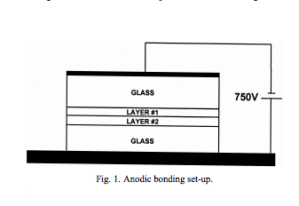
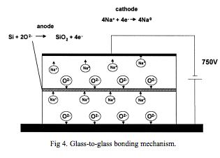
Planarity, materials, dopant concentration, applied voltage, and heating will all affect the strength of the bonds that form. We cannot polish the wafers after the membranes have been exposed, so we may be ultimately limited in the strength of the bond. I believe it will probably be good enough, as long as we do the best we can to bring the surfaces into contact (80% bonding is typical for CMP; I believe we will be fortunate to get 15-20%). The material system works fairly well for nitride to oxide according to the Materials paper. We will have to figure out a way to introduce Na+ or other suitable electromigration species into the thin films to provide the bonding mechanism (spin on glass + heat), being doubtful that residual contamination will do the job. Ideally, we would dope the spacer oxide layer before the free-standing regions are made, allowing us to use spin coating getting better uniformity across the chips. We can control the time course of the voltage and heating to get our best bonding using an anodic bonder setup:

There’s hope yet!