Modular µSiM Device Assembly
Introduction
We are aiming to make device assembly easy and quick, particularly for distribution to non-engineering laboratories. We are collaborating with ALine to develop assembly via pressure-sensitive adhesion techniques.
Assembly Process
Modular Device Assembly Animation2
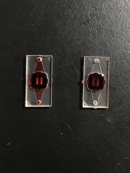
We made ten devices with porous membranes and ten with non-porous membranes to show no leakage.
Current Issues and Potential Solutions
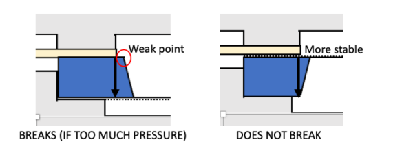
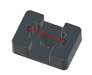
Old Issue: We found that often the chips break when assembling trench-down devices (trench-up during bonding), but are stable in the other configuration. We made slight adjustments to the components to avoid breakage.
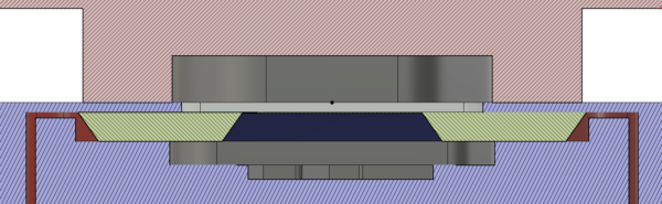
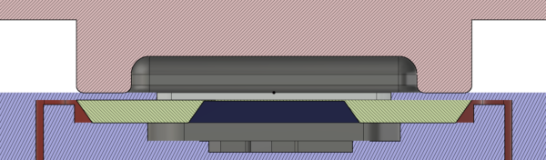
We also found that it could be difficult to add the top channel block into the A1 fixture due to pieces left after snapping off. We widened the middle of the A1 fixture so we can easily slide the piece in the component without forcing it or risking moving the chip.
I tested these modifications, however they still broke. Now breaking happened in either orientation. My wafer (1315) broke with much higher frequency than a comparable wafer I got from Kilean (1348).
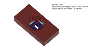
New Issues: Part of the issue was size/shape (more square, less rounding at corners) and the other appears to be weakness of this wafer. We need to adjust the top acrylic layer to accommodate size/shape differences, as well as the pedestal on the A1 fixture.
UPDATE
New modifications:
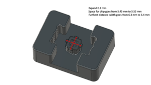
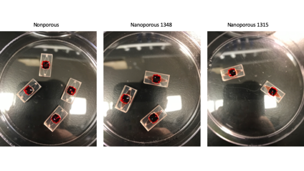
The ALine modifications came in and I tested them for breakage and leaking. We made 4 nonporous devices (2 trench up and 2 trench down), 3 nanoporous devices with wafer #1348 (2 trench up and 1 trench down), and 2 nanoporous devices with wafer #1315 (1 trench up and 1 trench down). Wafer 1315 has given issues before by breaking more easily and breaking out of the wafer bigger so they don’t fit in the top portion. With the modifications, however, we saw no breakage of chips or membranes. We had 9/9 successes with various people in the lab making devices, some with no prior experience in modular devices. You can apply a good amount of pressure with no issues.
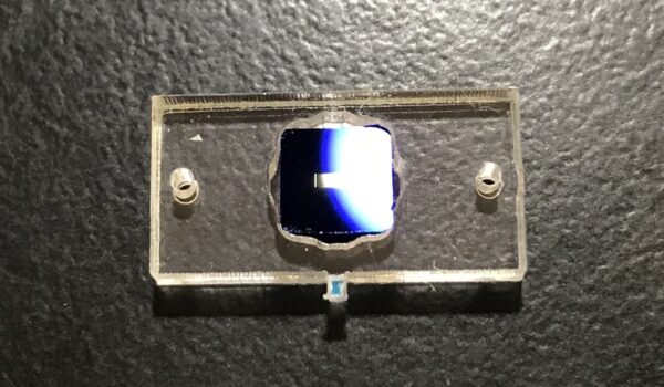
I did a leak test and the nonporous devices retained media in the top well and the nanoporous devices filled the bottom channel after 2 hours with no visible leaking.
Interestingly, when I checked the devices the next day, there was a difference in evaporation with wafer 1348 and 1315. 1315 had evaporated from the top and bottom, whereas 1348 was still wet in the bottom channel. They are supposed to be comparable in porosity and diameter.
Wafer #1348: NPN, 18-20% porosity, 44-46 nm avg diameter
Wafer #1315: NPN, 16.5% porosity, 46.1 nm avg diameter
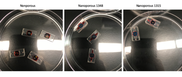
It is unclear why there are differences in the chips but it may be good to follow up with further characterization of the wafers.
Cell Culture
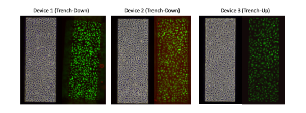
I grew HUVECs on three devices (two trench down and one trench up) and performed a live/dead assay after 48 hours of growth. All the devices grew cells with close to 100% live.
CONCLUSION
Modifications appear to work! We are ready to order.