SiO2 deposition – trial 2
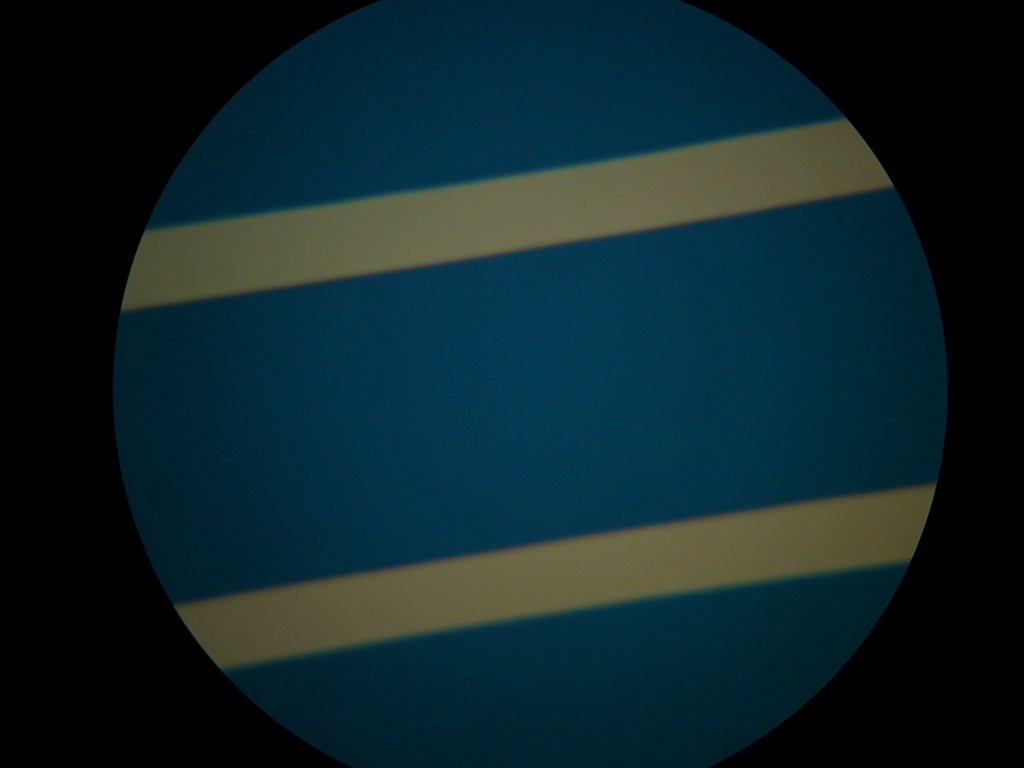
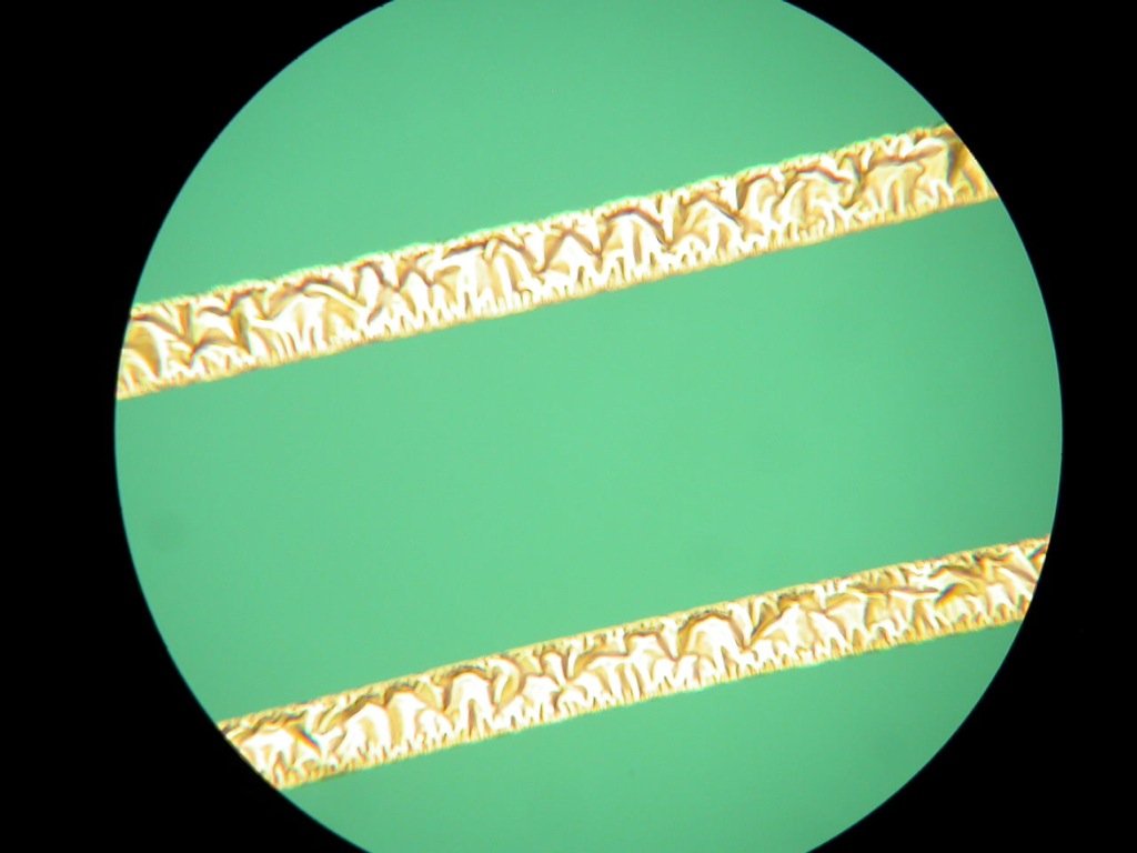
Last week, JP deposited 25nm SiO2 for me on wafer 644 (which I cleaned in the UV/Ozone before I gave it to him). Unfortunately, someone broke the E-Beam that day and JP was only able to deposit on 1 side of the wafer (the solid side). I did some experiments on the wafer anyway. First, I saw that the deposition changed the membrane structure from solid to wrinkled:
Before SiO2 deposition
After SiO2 deposition
I also looked at discoloration. Media was DMEM/F12 with 10%FBS.
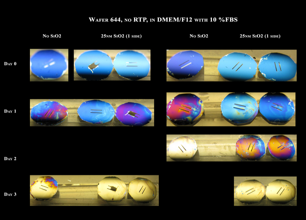
The 1-sided SiO2 didn’t slow discoloration as dramatically as the 2-sided SiO2 (past post). Not that surprising.
I then tried to image sodium fluorescein diffusion with the Zeiss. Here are images for time = 0 minutes and time = 20 minutes for unmodified w644 and SiO2 deposited. The membrane slit for 25nm SiO2 is just off the field of view. I couldn’t get the time lapse movies to post correctly.
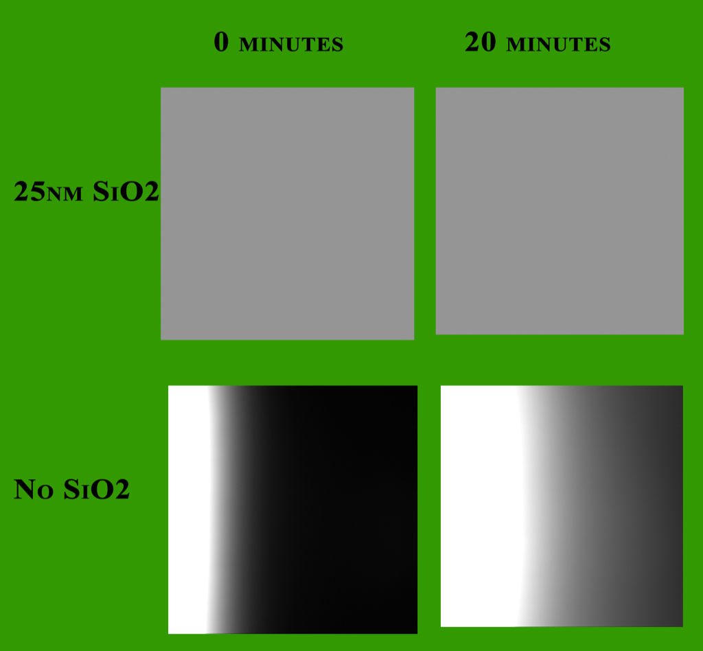
So it appears that there is no sodium fluorescein diffusion through the SiO2 deposited membranes, but there certainly is diffusion through unmodified w644. I’m still getting used to these experiments, so it’s possible that I didn’t do the set-up ideally.
I then took some samples to the AFM. This was the first time I drove the AFM on my own. I got some good images of unmodified w644 (top) and SiO2-desposited (bottom) chips.
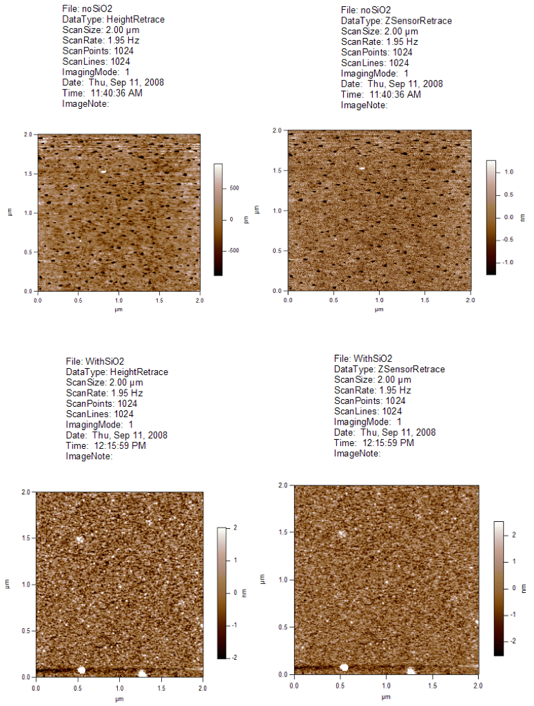
These are basically 2 different ways of looking at topography (the height and ZSensor scan). The nanopores are obvious in unmodified chips, and these images look pretty close to what we got with Keith a couple weeks ago during training. The pores are much less obvious in the SiO2 deposited sample, although some small ones are present. I’m not sure why the surface height is only ~ 2nm in those images. I can go back and get surface roughness for these if anyone is interested.
I would be more convinced that nothing diffused through the SiO2 samples if both time points were dark. You need to keep the camera setting fixed when comparing different conditions. Review with Jess or Tom if need be.
Haven’t we deposited SiO2 in the past and not seen wrinkling? If there was a problem with the evaporator, I would be suspicious. I’m fairly surprised that 25 nm deposited on one side can fill in all the pores, since they should not be particularly small on this wafer.
If you RTP the film, does it last much longer?
I’m not sure what happened with the SiO2 diffusion movies. I think the membrane slit is out of the field of view, so when I autofocused in TCGui, it wasn’t picking up the brighter membrane window. But since these are just images taken from a timelapse movie, the camera and microscope settings are the same.
Chris – I don’t know if wrinkling has been seen before or not. I remember that the wafers I did with Lingyun had wrinkled membranes but I’m not sure if they started out wrinkled. Can’t answer the RTP question since the machine is powerless (right?).