Double Sided Kapton Tape Affects MgF2 Evaporation Process
This week, I tried to make a large number of MgF2 nanomembranes for my collaboration with Kevin Webb.
I wanted to keep the evaporated surface as pristine as possible, so instead of using the Kapton tape to attach the chips to the platen on its face, I used double sided kapton tape.
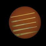
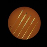
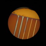
Our reserves of 1081 and 1085 nanoporous nitride that I had been using for my experiments had been running out, so I also switched to 1126 and 1127 nanoporous nitride chips (50 nm thick). 1127 has 18% porosity, and an average diameter of 41 nm, smaller than the 70 nm average diameter I had been using. When I first ran my evaporation process with the 1126 substrates, I used the double sided kapton tape and affixed them directly to the tape. An interesting film discoloration was present on a majority of the chips:
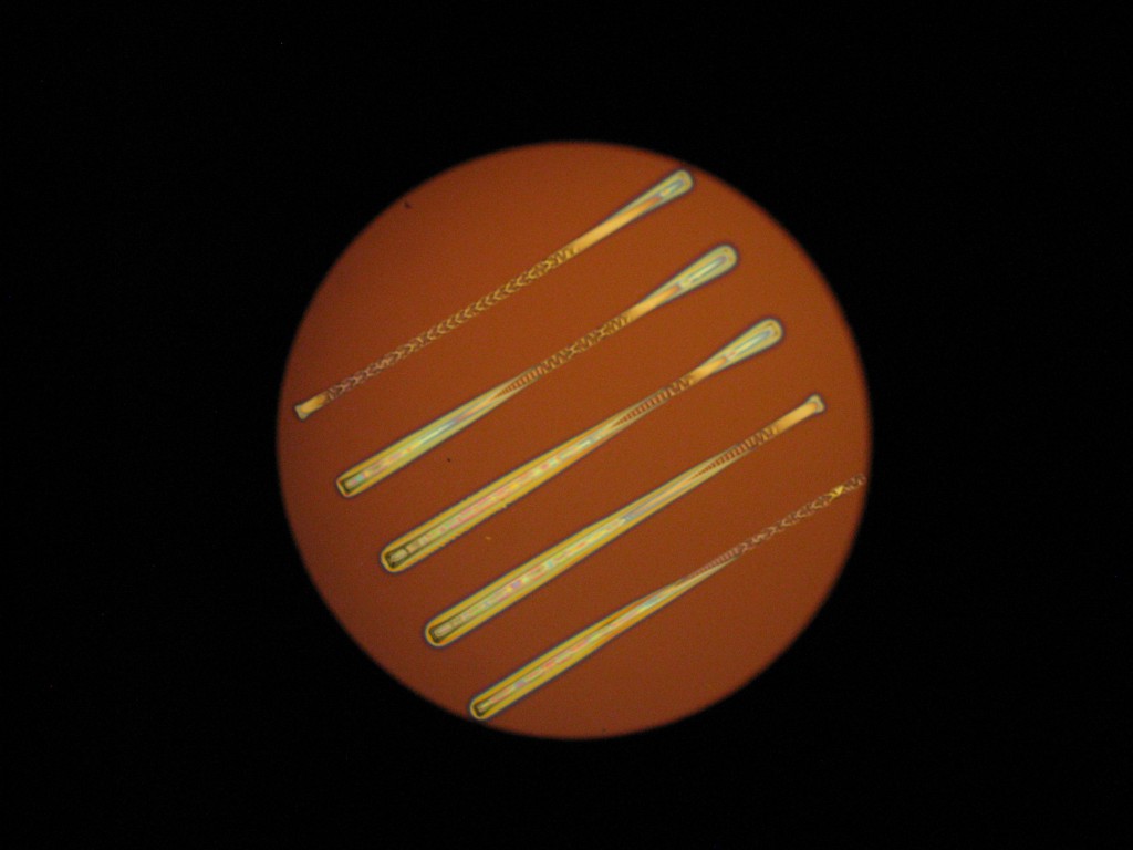

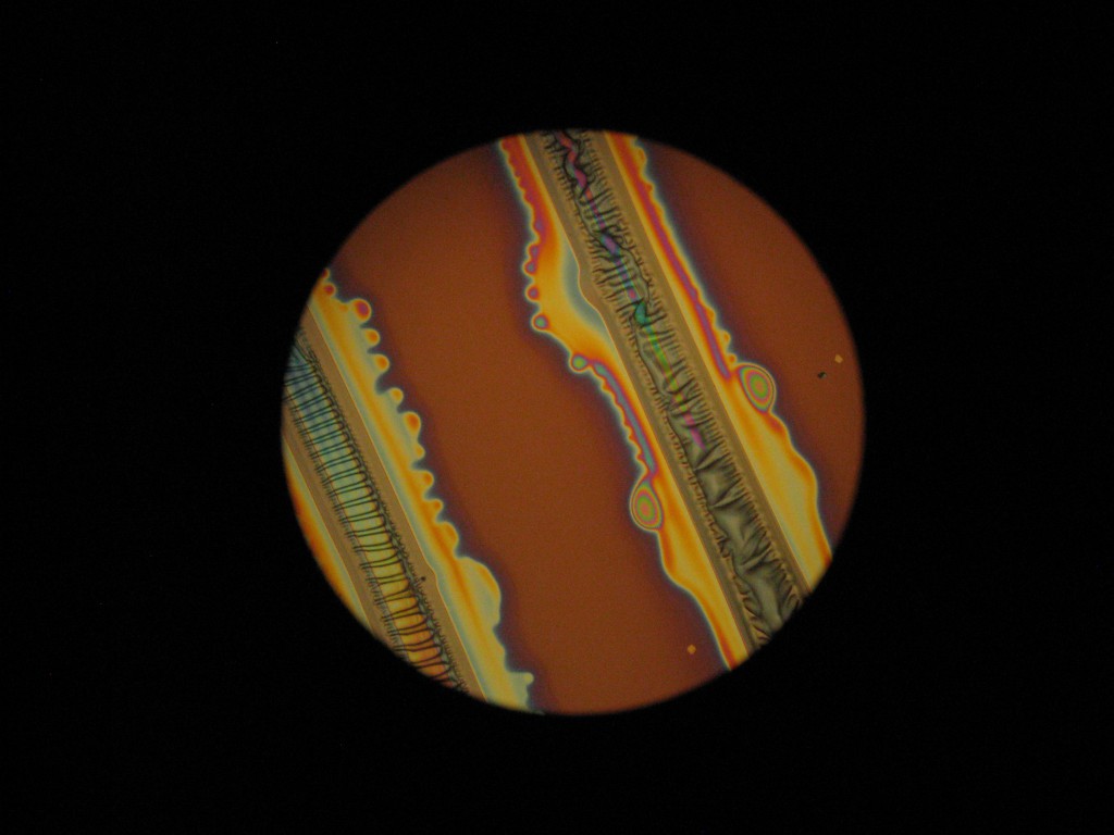
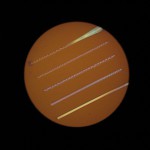
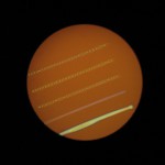
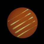
In a thin film, rainbow colors usually mean a thin film has a lot of thickness variation present, as the different visible wavelengths of light can interfere constructively at certain thicknesses (additional film or wrinkled film). I believe this to be evidence that the active areas in this evaporation do not have this same film thickness as in the bulk. Some of these chips had more extreme indications than others:

My evaporation metrics were normal (1-2.5 Angstroms/s, 250 C, 50 nm), so I was confident this result occurred because of the new tape or the new substrate. To that end, I did another evaporation, with different methods of fixing the individual chips to the substrate. I replaced the MgF2 in the crucible to make sure that a contaminated melt was not the source of this defect.


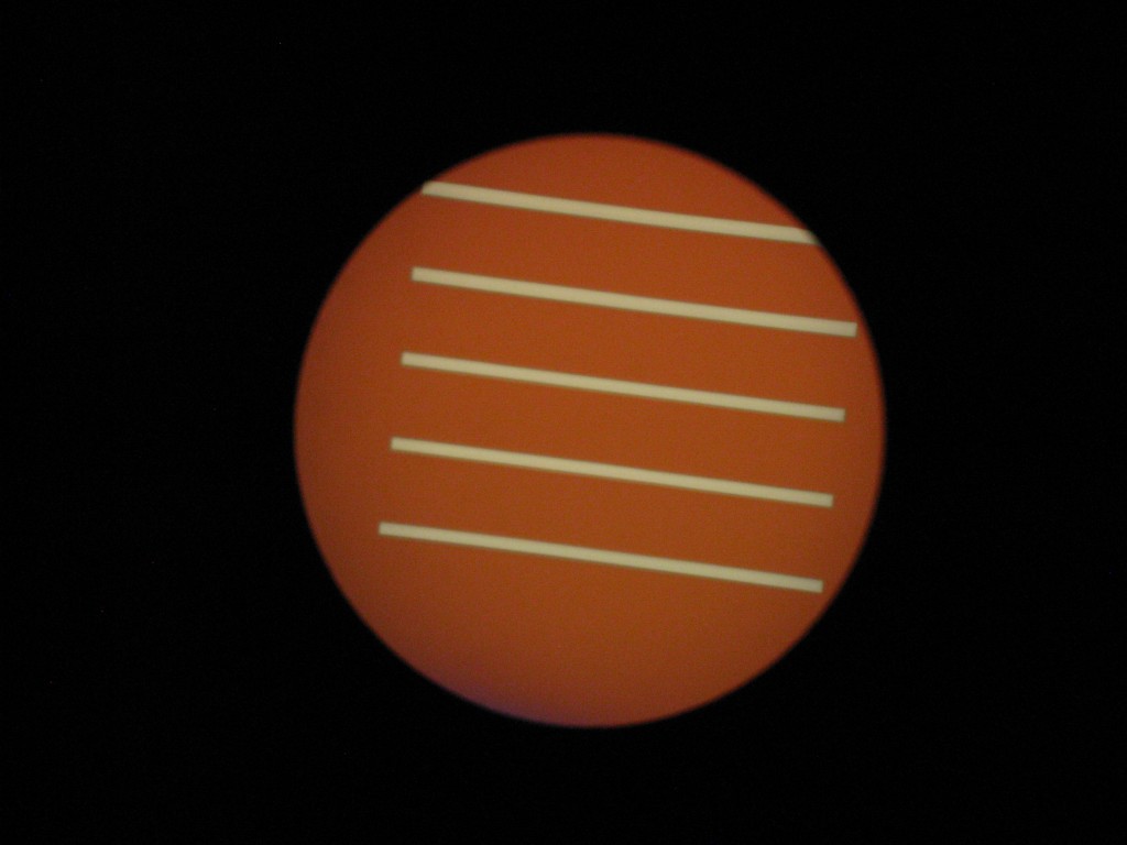
And my results are in:
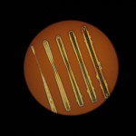
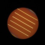
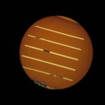
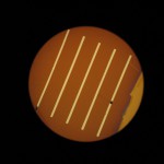
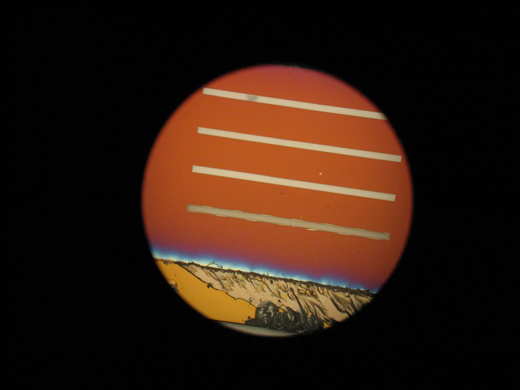
It’s pretty clear that something about the doublesided kapton tape is throwing off my process. It is possible that the tape is insulating the chips from the platen, meaning I get improper heating across the evaporation surface, or outgassing something terrible that affects the film around the active areas. The defects certainly appear worse as I switch to the suspended version compared to the bridged version. It’s not totally a wash though; even with the normal method, some discoloration occurs at the boundary (MgF2 could be delaminating from the Si3N4). With some of the normally affixed chips, it is possible to release some free standing MgF2 nanomembranes, albeit, not completely perfect:

In short, I believe that most of my problems were due to the new tape and not the substrate. I hope to confirm some of the defects with SEM, as well as verify the new pore distribution.