Silicon Photonics Integrated onto SimPore Chips
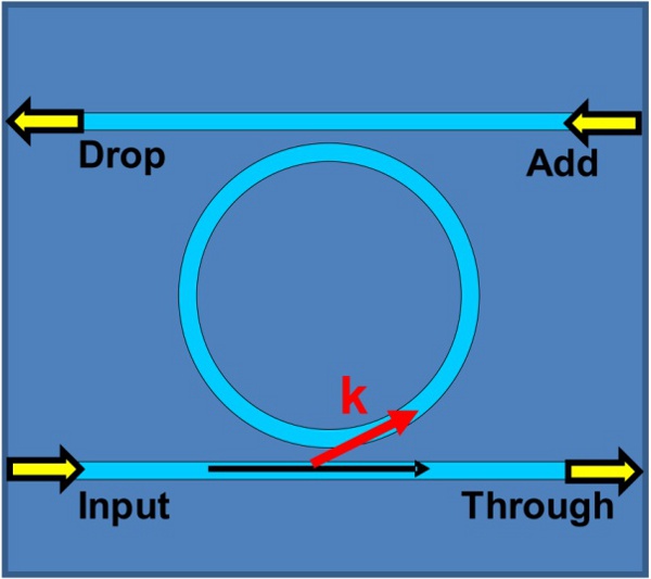
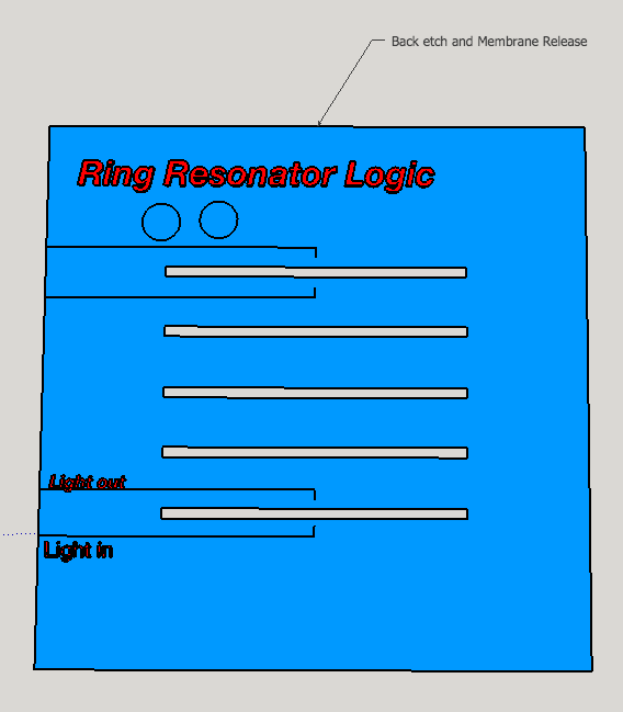
Ring Resonators are photonic structures that have a very repeatable behavior. As light is guided along a path, it can evanescently couple into a very closely positioned wire (submicron gap). If the wavelength of light is just right, constructive interference can occur, causing the rings to resonate (lost through scattering). Necessarily, this causes a drop in laser power across the rest of the wire. Incredible precision is possible with these interferences; 0.1 nm is enough to cause a substantial shift.

At BMES, I was intrigued by the increasing use of photonics in detection schemes, mainly for sensing concentrations of samples. Companies such as LuxTerra are producing hundreds of resonator rings on a single device. I thought we could potentially access these newer detection schemes by adding a silicon-on-insulator process to the manufacturing flow of nanoporous nitride.
- Form pnc-si on silicon nitride layer
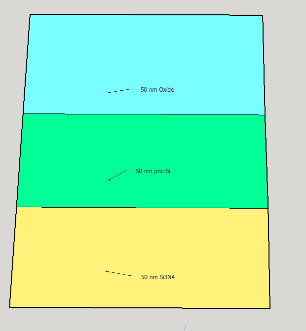
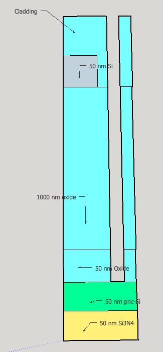
- Normally, we would etch the pnc-si pattern into the silicon nitride. Instead, we will substitute a silicon on insulator process that will allow us to fabricate photonic structures on the front side of the chip. We begin by depositing the insulating layer on top of the pnc-si. This layer provides the isolation necessary for confinement in the waveguide.
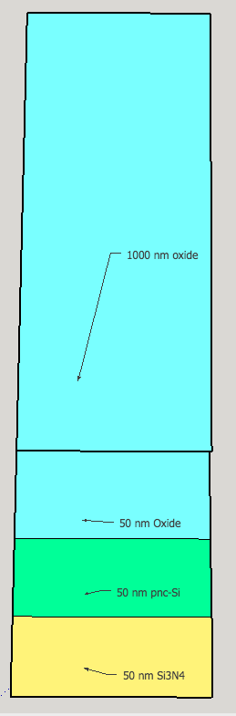
- We then deposit a layer of silicon on top on the insulating layer. This layer will form the photonic structures through litho/ebeam patterning
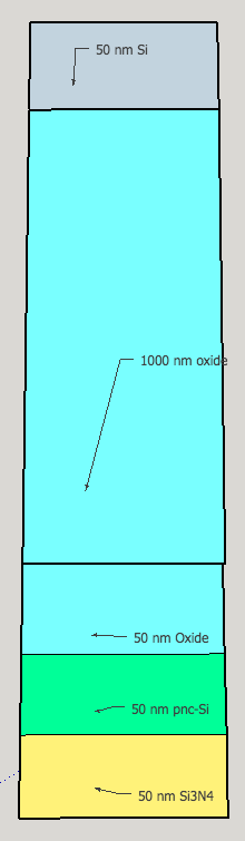
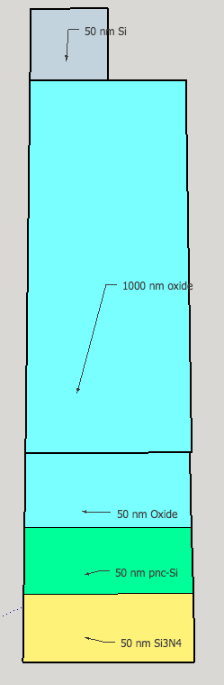
- Lithography/ebeam is used to transfer the photonic pattern into the silicon layer. The pnc-si is unaffected, sealed by the isolation layer.
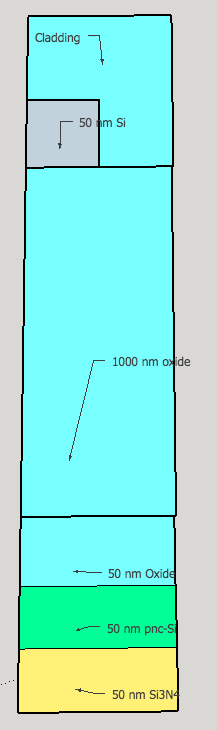
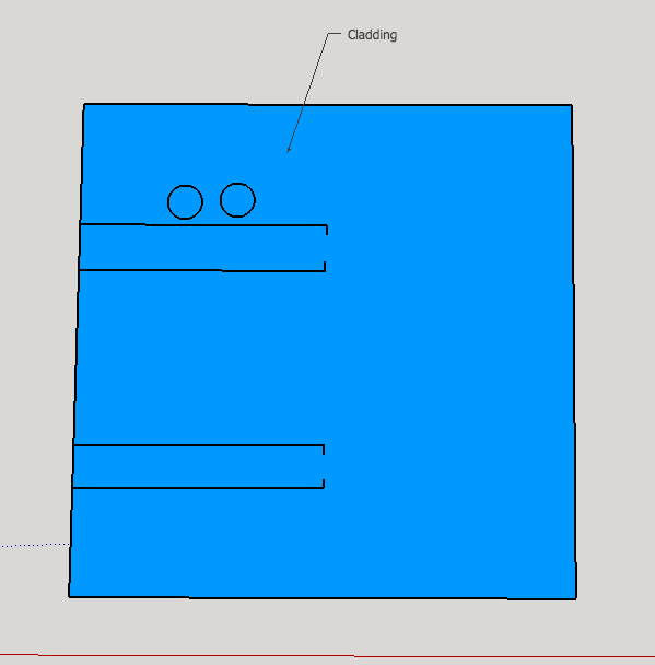
- We deposit a cladding layer on top of the photonic structure. This also allows us to tune the modes that enter the waveguides; different claddings optimally guide different frequencies of light. It is possible to skip this step too, but not ideal, due to possible modification of the photonic structures during further processing.
- We remove the cladding/isolation layers in what we would traditionally call the active area of the nanomembranes. This exposes the formed pnc-Si.
- We continue with the NPN process, transferring the pore pattern into the underlying silicon nitride film.

- Backside lithography + through-wafer EDP etching creates the traditional nanomembrane chip that we are familiar with.
If our attempts at Anodic Bonding are successful, the process becomes simpler because we can bond an arbitrary photonics chip onto/near a nanoporous filter.