|

Nanomembranes+Microfluidic PETLs Integration

Our collaborator Fernando has made a really nifty way to make microfluidics work with lamination pouches. These flat pouches can be sealed together using a heat activated glue, which can be done consistently using a 40 laminator (http://www.officedepot.com/a/products/404227/Scotch-TL-901-Thermal-Laminator/)     <span style="text-decoration: underline;"><em>Advantages</em></span> <ul> 	<li>If we could get our chips inside a flat system, we could really use vertical stacking to do some interesting microfluidic routing, weaving fluid streams in and out of chips.</li> 	<li>Cheap,15 for a 100-pack of 8.5″x12″ pouches + $40 laminator
  • Put multiple materials and multiple chips in the same microfluidic package. MgF2, NPN, Au nanomembranes of different pore size and material characteristics, electrodes, sensors could all be integrated in a floor plan, easily designed in illustrator or sketchup or even the silhouette studio software.
  •  

    Disadvantages

    • Likely not cytocompatible. PET doesn’t breathe very easily, and there will be many glue layers, which is not likely to be cytocompatible.
    • Resolution of channels is governed by the silhouette, not lithography. Micro tears and rough edges will not produce good results.
    • While optically clear, there are better plastics for imaging.
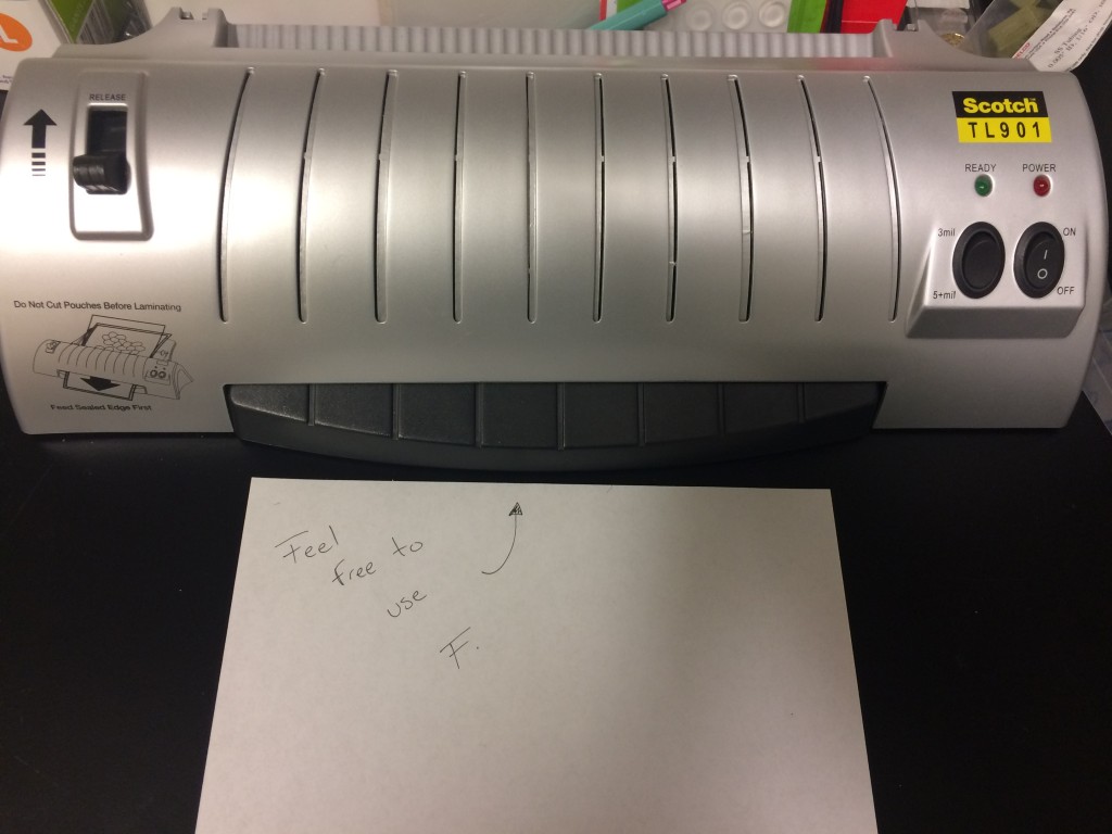
     

    The Laminator takes pouches, and rolls them through a heating element, fusing the glue on the inner surface of the pouch.
    The Laminator takes pouches, and rolls them through a heating element, fusing the glue on the inner surface of the pouch.
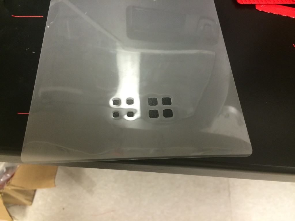
    Large pouches can be used and aligned to each other. I cut these patterns in half and aligned them to form a  'cartridge' for chips.
    Large laminate pouch, with glue on the inner part of the pouch. I cut these patterns in half and aligned them to form a ‘cartridge’ for chips.
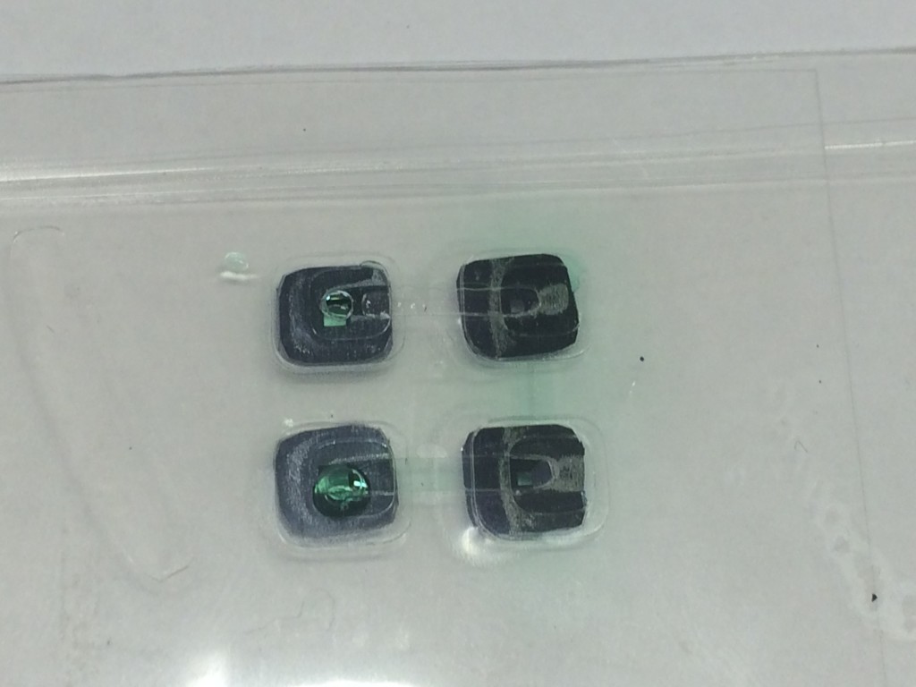
    8 layer device. Water routes across, down and back through 3 chips. Some in-plane leaking is observed around the top right chip.
    8 layer device. Water routes across, down and back through 3 chips. Some in-plane leaking is observed around the top right chip over time.
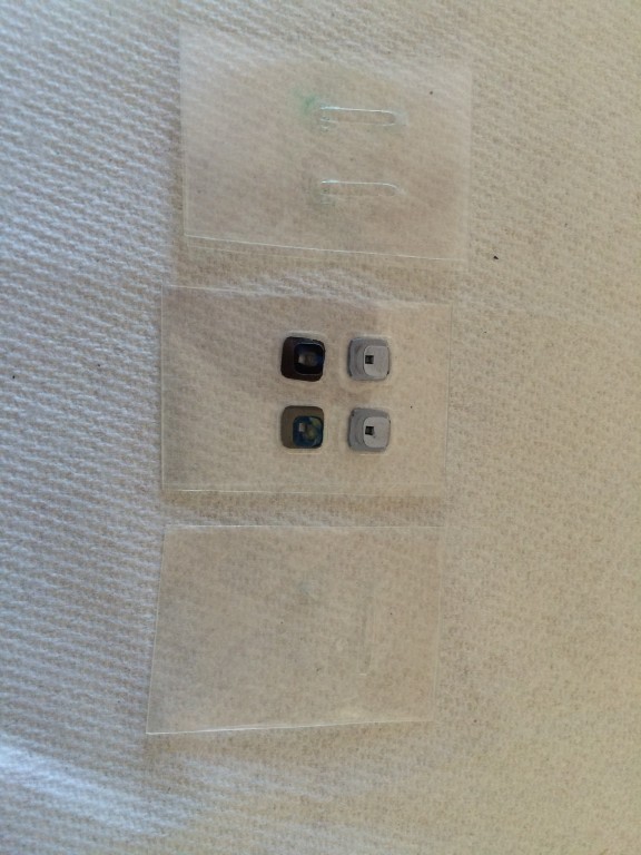
    The glue doesn't bond well as the number of layers are increased. This might be overcome with an oven-style laminator (microwave), which could more evenly heat the glue layers.
    The glue doesn’t bond well as the number of layers are increased. The middle layer is formed first (2 spacers+chip and a sealing layer), and then successive layers sandwich the middle structure. This might be overcome with an oven-style laminator (microwave), which could more evenly heat the glue layers. Also note the slight misalignment from placing a pouch within a pouch (middle object); everything has shifted by about 1 mm to the right.


    I find this approach to be very promising, even compared to gaskets. No soft lithography is necessary. No ozone bonding is necessary. The layer thicknesses are about 75 microns at their minimum. We can throw in foil electrodes where ever we like. I threw this together in an hour as a first attempt, from design to tested device.

    This will be an exciting space for us to explore further. The real key is to see if we can get the glue to bond to silicon effectively and evenly to each other as more layers are introduced.

    Similar Posts