Stabilizing the NPN pre-filter, and DNA results
I decided that instead of trying to figure out why it was delaminating, I would simply remove the option altogether.To that end, I painted PDMS on two NPN chips up to the oxide spacer.
Attempt 1:
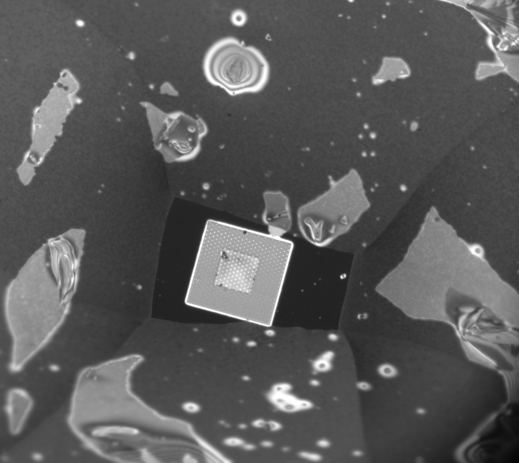
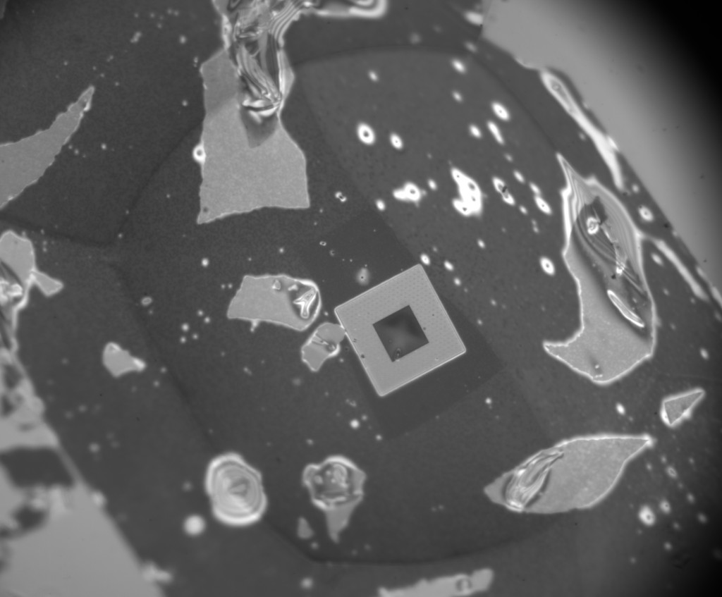
This chip was one I laminated myself using my breath to contact the membranes. In case it’s unclear, the region we see here has NPN everywhere, and the rectangle you see around the oxide spacer is the opening in the PDMS, which otherwise covers the entire 5.4mm square chip. The patchy areas of light color under the PDMS portion are actually bits of old NPN membrane, since this chip has been used for several laminations and cleanings at this point before I got such a nice transfer around the oxide spacer. Turns out it’s pretty easy to remove badly laminated NPN if the chip is hydrophobic (more on this later) by adding a drop of water and dragging it around on the hydrophobic surface, but it sometimes leaves behind a few bits that are a little tougher to remove, so I left them alone.
When curing PDMS I had to heat the chip to 80 degrees overnight to make sure it would not run into the open area. Doing so completely dessicated the membrane and made the NPN hydrophobic, so that when I put it in the freezer to condense vapor, all I got was large droplets forming on the surface, and no wetting of the holes in the oxide, which we can usually verify by watching evaporation of the water layer.
The membrane refused to wet initially (I believe Greg saw this same effect earlier).
To make it wet, I plasma cleaned it in air plasma for 60s at 60W, and the membrane wetted easily after that.
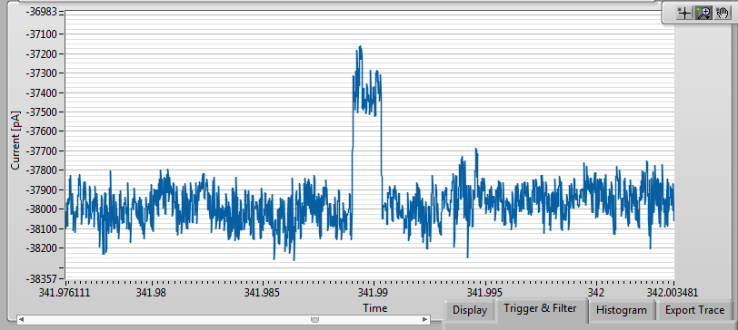
Fabrication of the pore was unremarkable, but the pore size grew abruptly during overnight conditioning to about 20nm, which is the upper limit for seeing DNA even in a clean pore, which this one was not:
I added DNA anyway, and captures a bare handful of rough events which are probably DNA, but there are not enough statistics to be sure:
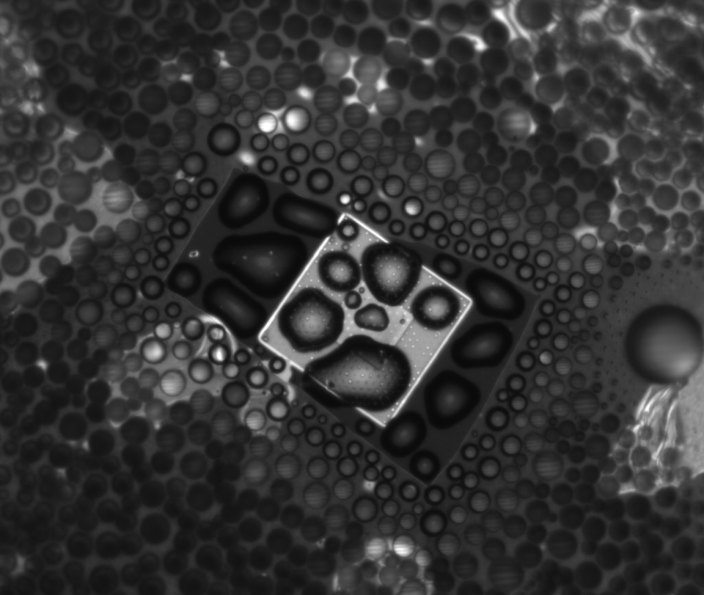
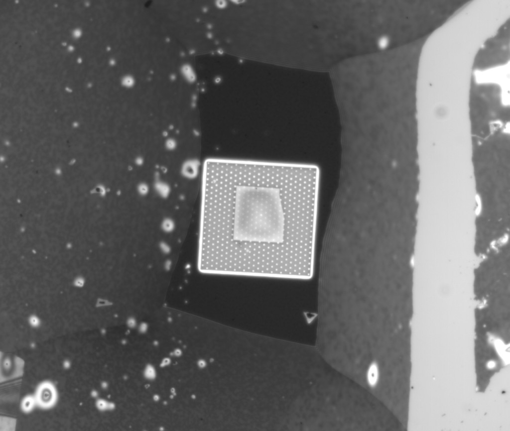
However, after taking it apart, the good news for this experiment is that after disassembly, the NPN stayed intact, as you can see below. The image is through water so it’s a little less resolved, but it’s clear that the NPN didn’t go anywhere. So that’s one more problem solved.
Attempt 2:
As before, this chip was laminated using my breath and steam to seal to the chip, which seems to work well about half the time now. I started by painting PDMS and cooking at 80 degrees overnight to cure it.
Plasma cleaning restored hydrophilicity, and wetting and fabrication proceeded normally. Note that during this wetting step there was some ambiguity as to whether the vapor condensed properly in the freezer, but after adding a droplet of liquid on top everything worked well. I am starting to think we might not even need the freezer step, and that simply wetting the outside of the membrane will take care of the inside region as long as it is hydrophilic.
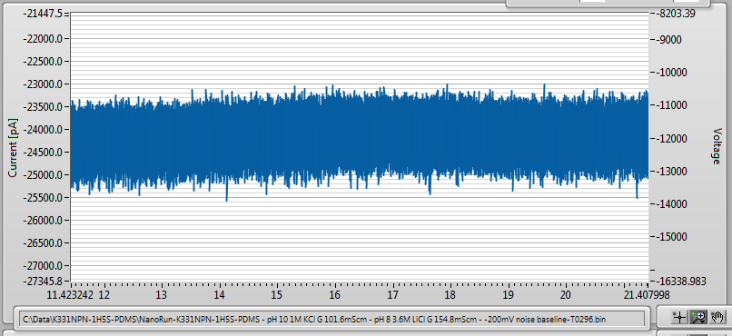
In any case, fabrication went normally, and after leaving it to sit overnight to improve the noise characteristics, I ended up with a very, very low-noise 10nm nanopore:
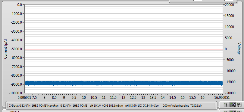
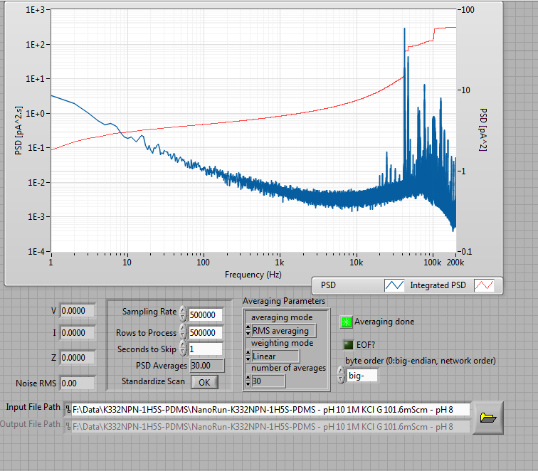
After adding 21nM 2000bp dsDNA, I saw this, at -200mV applied bias:
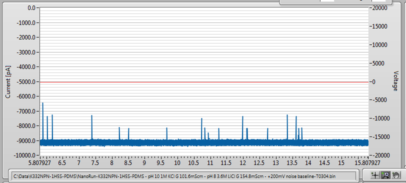
It works! And what’s more, this event rate is not too much lower than I would expect for a pore without NPN. So it seems that if the membrane stays laminated and the pore is sufficiently well-behaved, the NPN present very little barrier to DNA passage, at least at this size scale.
To make sure the NPN was still there I took it apart for imaging, and sure enough:
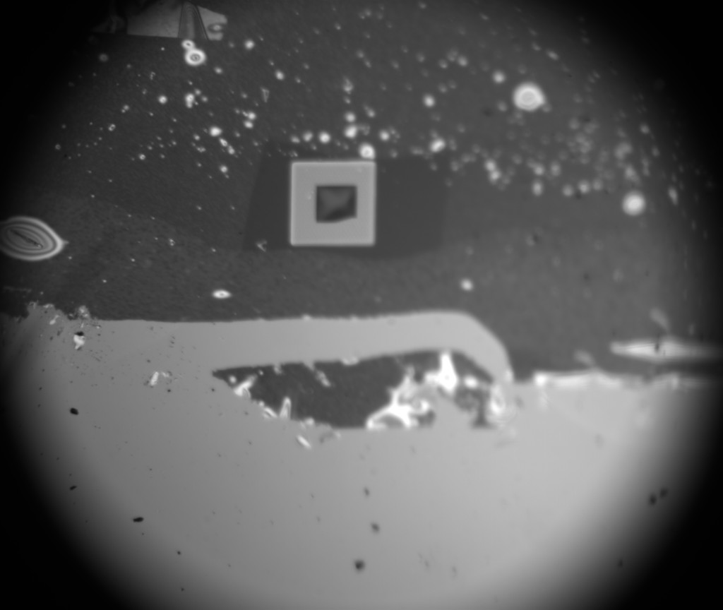
So, while i don’t think it’s possible to rule out a crack in the NPN layer from optical images, the fact that this is a 1um hole/5um space chip with a pore in a single oxide hole makes it rather unlikely, so I am confident that this is the real thing, finally.
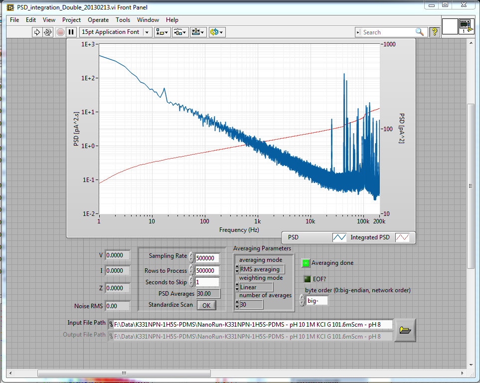
Analysis of the DNA results gives the following statistics:
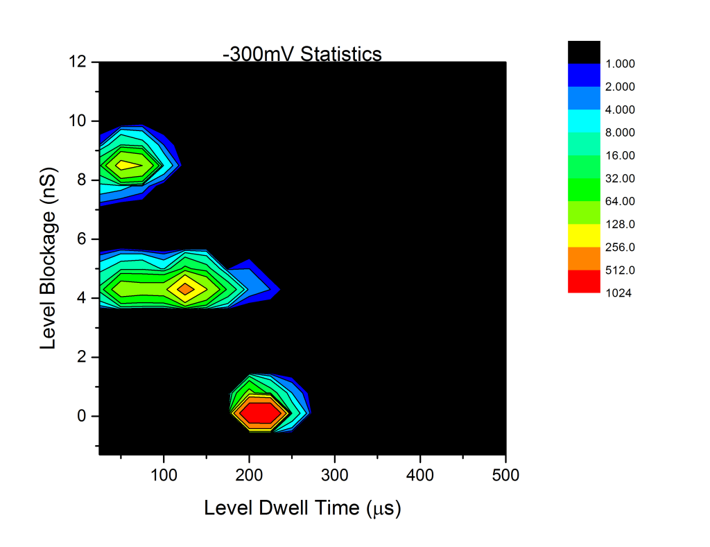
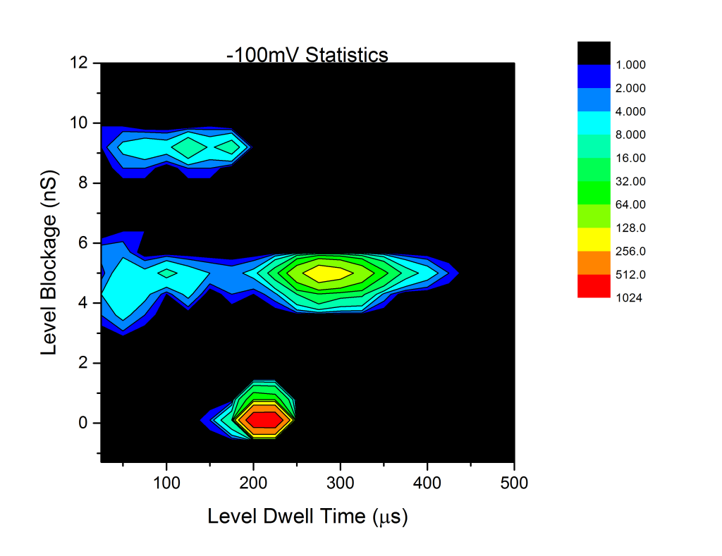
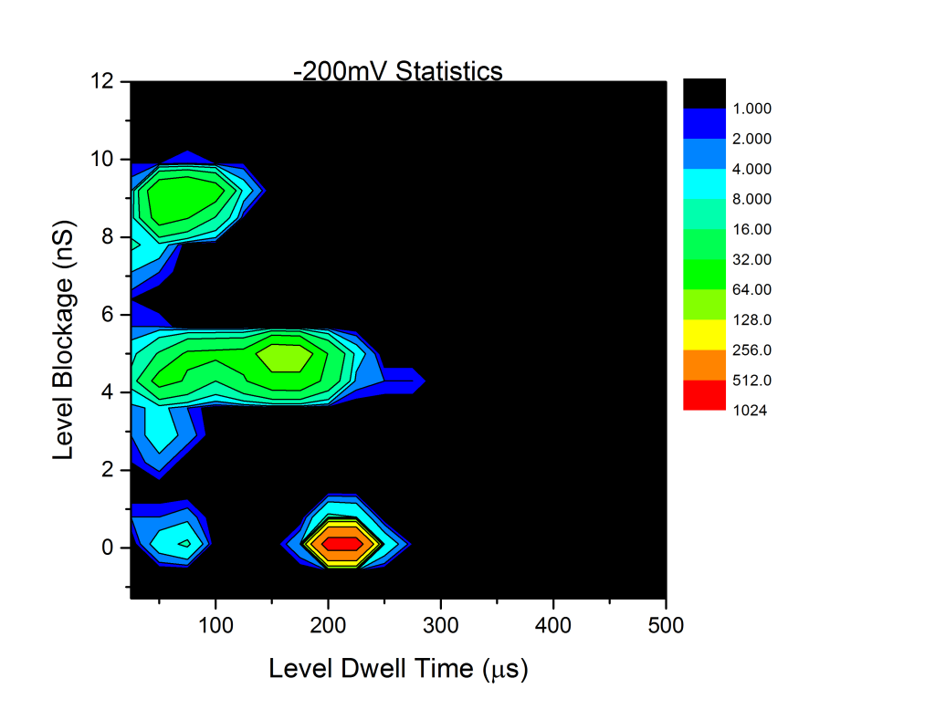
The peaks around 0 blockage are the baseline padding, and the other two peaks around 4.4 and 8.8nS are the single-file and folded DNA peaks we expect. Note that the color scale is log2. Using the equation

We can extract an effective membrane thickness of 
Also noteworthy is the tight dwell time distribution for the various levels, which (at first glance) has fairly low spread. I won’t speculate too much based on a single pore, but if we see that consistently with smaller pores as well it could be an interesting effect by itself.
So, this experiment by itself doesn’t show much about the filter (electrically, you can’t even tell the NPN layer is there at all), but it is an important step since it proves that DNA can go through the NPN layer even in the absence of significant electrical bias. It is possible that the NPN does reduce the voltage across the pore, in which case we would have systematic errors in our calculated pore size, but without some modelling I can’t say for sure. Something to think about for the paper, when the time comes.
On other fronts, we have had a handful of nano-particle experiments in regular membranes that showed a few blockages, but they are very short. Because of the thin membranes we use, the dwell times of nanoparticles is just a few microseconds, so it’s likely that we are getting tons of events but simply can’t resolve any except the extreme outliers with our system, and even then it is badly distorted by the hardware filter. I will continue trying to get those running, but we may need to approach the size separation differently, perhaps with bulky tags on DNA or something like that. I also expect that longer DNA will have a harder time getting through the NPN. Because there is almost no bias, there will be an extropic barrier to passage once we get past a few thousand base pairs which might allow us to pass short DNA but not long strands. Time will tell.
Two things we know: Delamination issues can be solved with PDMS, and DNA can get through the NPN layer without negatively impacting the quality of results.
Very encouraging progress! A few scattered comments:
On wetting, yes we saw trouble getting the membrane to wet initially after thorough desiccation. Typically we just breathe on it several times in succession and it begins to wet again as normal. I agree with your contention that the freezer step could be unnecessary — we’ve had plenty of success without it.
In experiment 1, you say that the pore grew overnight. Can you briefly explain what that means for us? The device is worse off, but does this problem indicate an issue which could possibly be due to the nanoporous filter or the tenting process? Not familiar enough with your single pore drilling process.
Finally, in experiment 2, is the information you captured enough to recover the sequence of the DNA which was fed through the pore, or are we not there yet? The low noise is exactly what we were hoping to see with the addition of the filter (in addition to, as a consequence of that, improved device longevity,) so that’s a really great result. It would be compelling, I think, the compare average noise levels between protected and unprotected nanopores of similar size.
Re: growth, we use intermediate voltages applied to the pore to increase its size. Usuually this is a very slow and well-controlled process, but occasionally a pore will have some instability and it will grow suddenly and we miss our intended mark (<5% of the time). That's what happened here, it has nothing to do with the NPN, and at the moment, there's nothing we can do about it since it is most likely to do with the membrane quality immediately in the vicinity of the pore, which is not something we can control yet.
Re: sequencing, solid state nanopores cannot yet sequence DNA at all. For a 15nm membranes, there are ~45 bases in the pore at any given time, so the signal we recover is a convolution of 45 base pairs, so there's no way to recover sequence information. A few groups (and Oxford Nanopore) claim to be able to do it with biuological pores which have a thickess that allows for only 3-4 bases in the pore at a time, which simplified the statistics required.
The low noise actually has nothing to do with the NPN layer – it's all about the PDMS, since noise comes from capacitance, which the PDMS reduces. If anything, I would expect the NPN layer to add noise to the system, but if it does, it's too small to be noticeable. The NPN does not actually change the noise characteristics measurably, which really is a best case for us.
Very practical, well done. In the end, your structures were not stabilized by vapor alone, but PDMS creep didn’t appear to be an issue. Your use of a meniscus to ‘sweep’ away the debris was very clever! I have a few questions/comments, but they are mainly my curiousity.
1. I have seen previously that if the tented structures were given time to dry out completely (dessicate in oven), they did not wet, much like you have seen here. It’s really great news if the ozone can ‘reactivate’ a device, without repeated wettings. That’s something that could be tested in one of Henry’s sealed devices.
2. Pores change shape after the dielectric breakdown events occur. Is it mechanical weakness that sands away the edges of the pore? It would make sense if the breakdown caused additional damage near the edges, and the flakes simply didn’t dislodge immediately. I recognize it’s not a frequent occurrence.
3. How much did the noise improve from leaving it overnight? Is there room for improvement for minimizing the ‘seasoning’ time of the device? If so, that might be something to consider for another device structure. The PDMS acts as a low capacitance film, thus it begins to dominate the behavior, but are there other implications here? Is it going to be removing precious solute from solution? If all we need is low capacitance films to smooth out the noise, that is something we might be able to fabricate.
4. The event rate was lessened somewhat, but that is ok if the device runs for longer periods of time. How long was the device in operation? If it isn’t substantially longer, it may indicate that the membrane is too close to the nanopore, and not really doing a filtering/straightening job.
5. I remember a 15 nm nitride film.
6. Vincent did some calculations early on about the electrical properties of the NPN membranes with regard to the DNA ‘sensing’ the fabricated nanopore. Maybe the electrical drop of the nanomembrane calculation has already been done?
7. I’m really excited to see the longer DNA chains.
8. It would be interesting to see what kind of aggregates/junk are caught on the tent from an actual dsDNA translocation run would look like. If you save some of these, we might be able to do some TEM to look at them. I’m thinking it might be possible to actually visualize the nanopore through the tent on top, but I don’t know what the depth of focus on the TEM is anymore.
9. A random thought, but does the dielectric breakdown fabrication method work with graphene? I don’t see a good reason why it shouldn’t in an ideal film, but I can think of a few bad reasons, where the graphene deposition defects dominate the placement of your lightening bolt. I read that a graphene-thin pore could potentially sequence base pairs, but I’m not a believer because they’ve been poking holes in the film with a FIB.
Meliora et Excelsior!
1 – yes, the plasma seems to reactivate the wetting surface. It’s also very gentle, and there is no optically visible change to the membrane.
2 – We really don’t know what causes stability issues of this nature. We have noticed that batches of membranes from the same wafer tend to have similar stability properties so it seems like it is a material quality property more than anything. However, the issue I saw here wasn’t instability in the pore size over time, rather an abrupt growth, which happens but is much more rare. It could well be damage to the edges as you suggest, but we have no way to test that at the moment.
3 – Noise varies from pore to pore – many pores work and behave nicely immediately. This one actually was pretty good already, but I wanted it to grow a little bit and I didn’t want to use voltage to condition it given what happened to the last one, so I decided to leave it and let it grow a bit naturally, which is a pretty common thing.
Regarding noise, the main role of the PDMS here is to stabilize the NPN layer, which otherwise has delaminated in all of my experiments. The noise improvements are a happy coincidence – one that can certainly be done using an oxide layer in the fab, but we would still need PDMS to seal the NPN layer.
4 – the device didn’t fail during the run, which went for several hours. What ended the experiment was the need to go home and eat dinner, and the file sizes generated are too big to leave it overnight. I am skeptical that we could reliably show device longevity improvements systematically, however. The statistics necessary would require 10s of successful devices and as many controls because of high variation. It’s doable in principle, but it won’t be fast.
5 – perfect
6 – It’s pretty simple to do a rough ballpark based on pore conductivity. The drop should be small, in any case.
7 – I think we will start to see a drop in event rate for longer chains as the entropic barrier to NPN passage grows. This might be a good way to show size exclusion without labels if the nanoparticles don’t work out.
8 – Good luck finding the nanopore ^_^. But I can certainly dry out and store the successful devices. I tried to flush this one out to try longer chains but the pore grew during flushing of solution so it didn’t work out, and any debris probably got flushed away. I wouldn’t expect much, the sample I added was very clean. We could try to use a dirty sample and see if it still works by adding some contaminant of appropriate size, if you have something in mind.
9 – Yes, it does. Golovchenko’s group at Harvard have used CBD to make pores in graphene. Harold Kwok tried a few integrated graphene devices before he left, but we moved away from them, mainly due to the difficulty in obtaining good quality graphene. All of the literature I have read about graphene suggests that while in principle it should be able to get close to the sequencing limit, it is actually much noisier than nitride, which is currently the limiting factor there last I heard.
woops, wrong reply button