Final COMSOL Analysis to Interpret TEER values from pncSi Transwells
For last 1.5 years, I have been working on developing a COMSOL model to understand how the geometry of pncSi chips affects the TEER values when cells are growing on them. I addressed this issues in some of my previous blog posts. What was lacking in the previous post (which I thought was the concluding one) was the validation of my model. Having a consistent FEM model without any experimental validation is not sufficient. So I revisited and redid most of the analysis along with experimental analysis to understand how electric field lines inside a transwell insert having pncSi chip behaves. So I will to systematically explain the problem, the solution and take-home in this post.
Problem
Barrett performed lot of experiments in establishing BBB on pncSi chips in a static system. TEER was measured using Endohm chamber connected to EVOM Voltohmeter. The resistance values are multiplied with membrane active area to yield the values in ohms-cm^2. The raw data is as below.

There is a lot to take in this graph. There are two axes to begin with. The red lines belong to the left axis and represent raw resistance values in ohms. The blue lines belong to the right axis and represent the normalized resistance in ohms-cm^2. The dashed lines represent the data obtained from pncSi-membrane transwells. The solid lines represent the data from commercial PET-membrane transwells. As we can see while raw values on pncSi (~400 ohms) are about ten times higher than the ones on PET (~40 ohms), the normalized values follow the opposite trend (13 ohm-cm^2 on PET vs ~1.5 ohms-cm^2 on pncSi). This discrepancy is because of the difference in the geometry of the two membranes’ active areas. The PET membranes has its entire cross-section porous, while for 2-slot pncSi membrane it’s barely 220.1/33 = 1.2 % porosity. This reduction in permeable area causes the field lines to bend across the porous regions and add an extra ‘path’ to the current streams, thus explaining the higher raw resistance values. The COMSOL model can explain this phenomena. The model schematic and simulation results look like below.


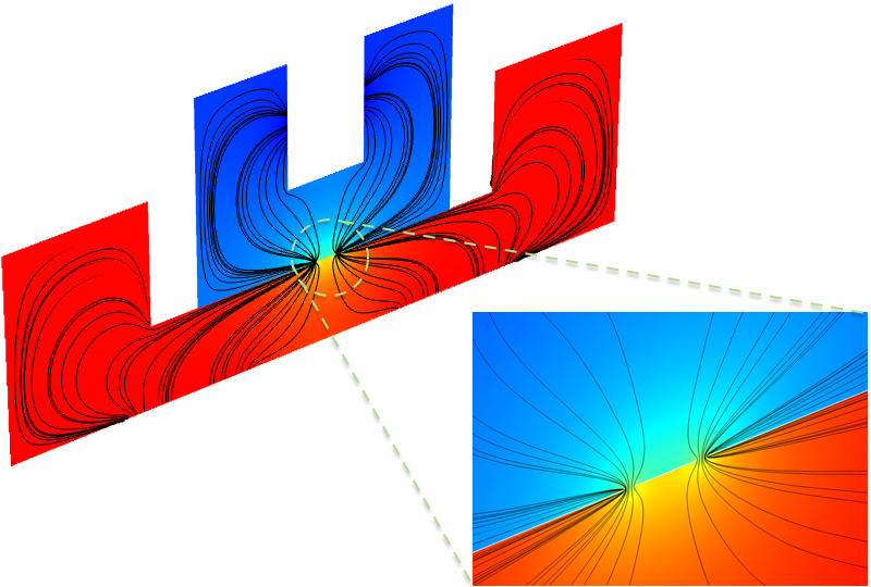
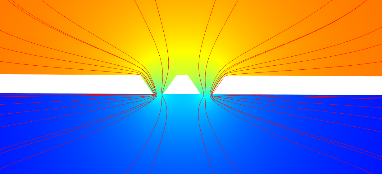
As the field line diagrams suggest, the lines through a PET membrane are more or less completely orthogonal to the membrane with negligible bending. For the pncSi membrane the constricted geometry of the porous region makes results in bending of the field lines causing an increased resistance value.
I further tried to model the cell growth in Comsol and see if we can predict the TEER values on the different setups. I used a biphasic growth curve as published by Jim’s previous grad student Mike Bindschadler. It allows us to account for contact inhibition in the cell culture. The cell density was 50000 cells per cm2, and assuming a cell size of 50×20 um2, I estimated that the initial cell density was about 50% of the total population a transwell can hold. Contact inhibition was introduced when the cells reached about 90% of the total capacity. The termination density was 97% for the pncSi model, and 99% for the PET model. Using these growth conditions I predicted following two curves for the two transwell-systems.

The graph on the left predicts the growth curve on pncSi membrane-transwells, while the one on the right predicts the same for the PET transwells. As we can see, simulation growth curves match very well with the experimental ones, especially near the confluence. Error bars are S.E.M with n=3-5. The mismatch during the initial stages of cell growth might be attributed to the assumption we made that cells grow uniformly over entire membrane area, rather than island patterns [principle of superposition]. The match near the later stages confirms that once the cells are confluent and cover the entire region, this assumption is accurate.
The overlapping of the growth curves in the case of both commercial transwells and custom-designed inserts also act as a validation of the FEM model and further proves that the cell growth although behaving similarly in two systems can generate apparently different resistance values. In order to resolve this apparent discrepancy between the values, it is necessary to engineer a mapping function or a transfer function that can correlate the different values amongst the systems, which can allow the researchers to use either of the systems without losing the reliability of the values. The simulated curves in each of the above graphs use the cellular resistivity as a common input parameter. Identical cellular resistivity values however result in different final observed resistances due to geometrical artifacts. However, the apparent and the actual resistance values can be tied together due to their common origin in the modeling, and can be interconnected with each other while eliminating the independent input variable of cellular conductivity.

As explained earlier, the raw resistance values obtained from the systems using silicon membranes cannot be straight multiplied with their active permeable area to yield normalized TEER values. The transfer function, however, can allow us to map the values from the silicon-based transwells to the commercial systems. The ‘mapped’ resistance values can then be multiplied with the area of the transwell insert (0.33 cm^2 in this case) to report the final recorded TEER values in ohm-cm^2.

For example, if the resistance value recorded by the Voltohmmeter while using a transwell consisting of chip-based silicon membrane is 1200 ohms, the actual resistance established by the cell layer would be around 60 ohms if a commercial transwell was used. Following this conversion, the TEER value reported will be 60*0.33 = 20 ohm-cm^2.
It needs to be noted that this mapping function is only applicable to the system modeled in the paper. Any changes performed in silicon membrane geometry, lithographic patterning of the permeable regions, the type and geometry of the electrodes used etc. can change the electric behavior of the system drastically and will demand a different mapping function.