Production from 12.06.2007
This week’s production included wafers of antimony (Sb) and phosphorus (P) doping.
Process parameters
The deposition heater was re-brazed prior to this deposition. We were concerned with the original brazing job because there were areas with “globs” of material and cracks in the solder. The new braze covers most of the surface, and although is not perfect, does not seem to outgas any contaminants or affect vacuum performance. All wafers were held in place with a solid stainless steel backing plate (to help with temperature uniformity during the dep.)
Wafer 312, 313
- P-doped
- deposition @ 400C
- 950C RTP
Wafer 189, 190
- Sb-doped
- deposition @ 400C
- 950C RTP
Wafer 310, 311
- P-doped
- deposition @ 400C
- 975C RTP
Wafer 187, 188
- Sb-doped
- deposition @ 400C
- 975C RTP
Details on the front-end processing can be found here: JP’s flow
Pinhole density was low across all wafers, and yield after the full-wafer strip was close to 90%.
Images
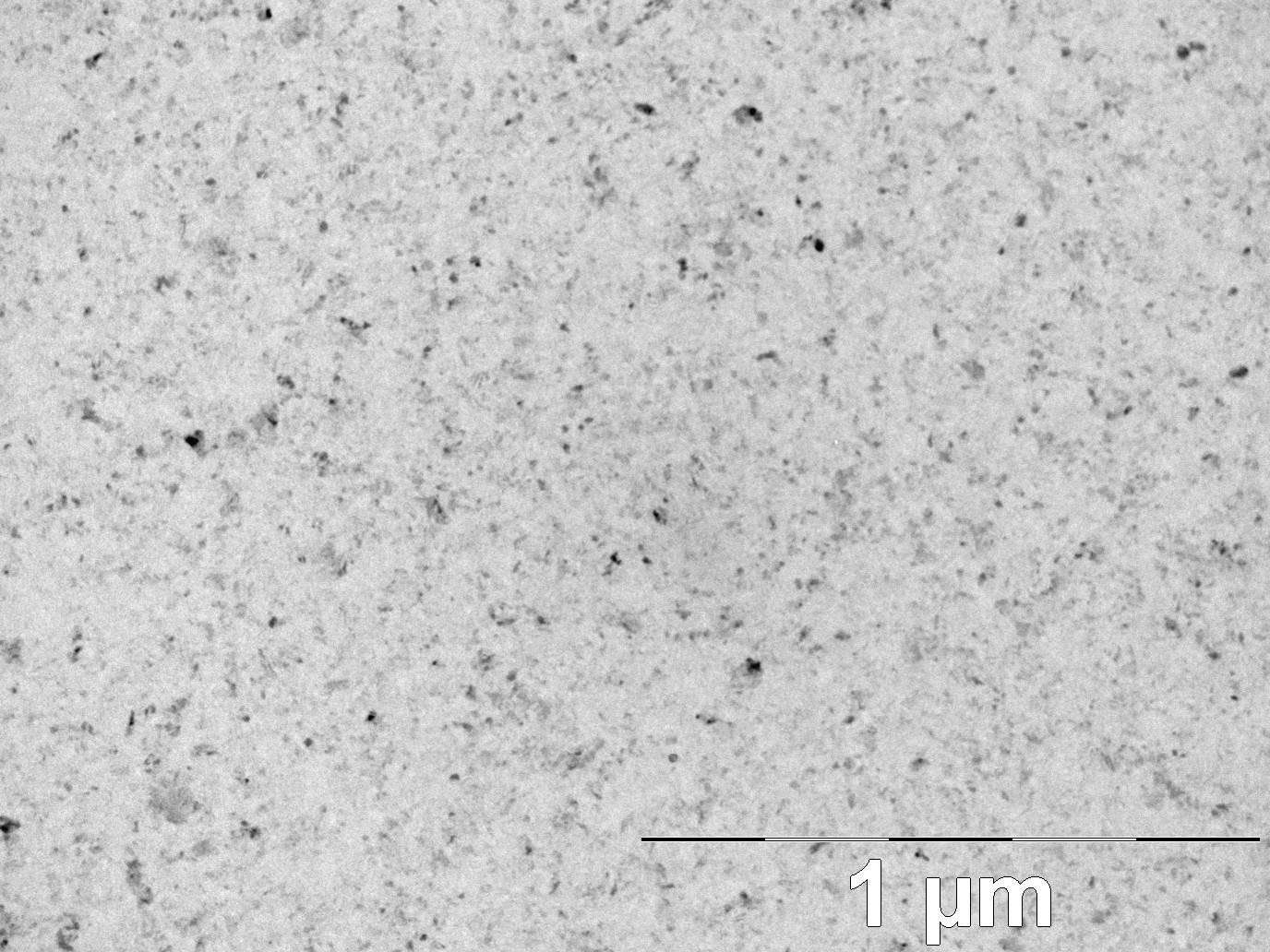
wafer 187 – Sb – 975C RTP
 (0,0) @ 50kx
 (0,-3) @ 50kx
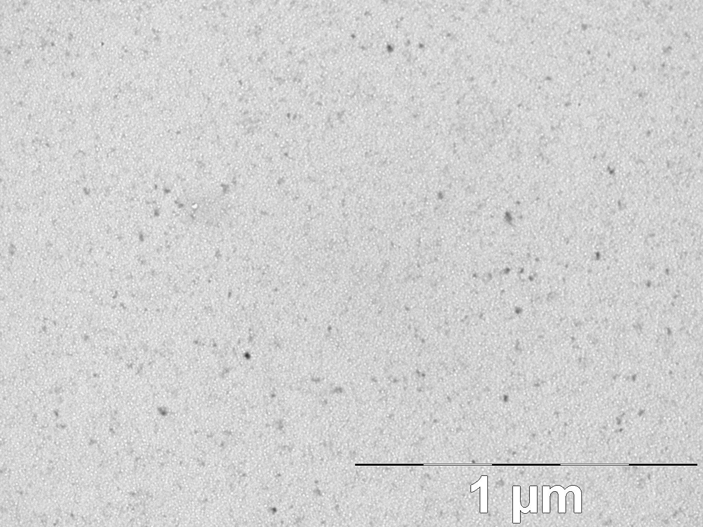
wafer 189 – Sb – 950C RTP
 (0,0) @ 50kx
 (0,-5) @ 50kx
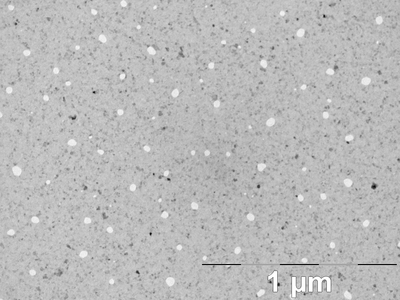
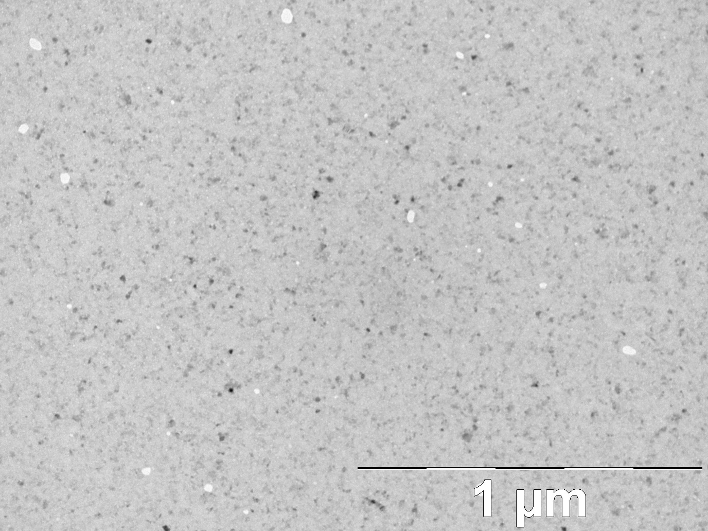
wafer 310 – P – 975C RTP
 (0,0) @ 70kx
 (-4,0) @ 50kx
wafer 312 – P – 950C RTP
(0,0) @ 50kx
 (0,-4) @ 50kx
A few trends to note: 1) there is still a pore distribution non-uniformity across the wafer 2) the P-doped wafers seem to have larger pores as compared to the Sb-doped wafers.
It is very possible that the Sb/P wafers are seeing different temperatures in the RTP, since their optical absorptions differ (see Maryna’s figure below). In other words, the pyrometer in the RTP is seeing different temperatures as the energy passes through the wafer, which changes the feedback in the control system.
The Sb wafers are much more absorbing in the IR.
 wafer 310 (-4,0) @ 300kx
Lastly, the low-accelerating voltage TEM at URMC is giving us much better contrast in the images. The image below is interesting because there is a defect structure (microtwin) close to the center pore that stops abruptly at the lighter “ring” surrounding the open pore. The take-home is that our pores are “coated” with a different material. Oxide? Amorphous Si?
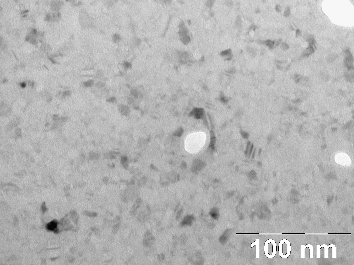 wafer 310 (-4,0) @ 300kx