Production from 1.10.2008
Last week we processed wafers 335 – 340. Our goal was to track down the source of Cu contamination. We sputtered membrane films both at room temperature and at 400 C. Our thought was that the RT dep. would not show contamination if the sputter heater was indeed the source of our Cu. It turns out that all the wafers had a presence of copper, although the wafers that were deposited at 400 C had a higher density of particles. This week, we removed the sputter heater completely from the chamber and ran all depositions at RT. Those results will be up by early next week.
Be warned that wafers 335 – 340 show “tears” that are most likely being caused by these Cu particles (the dark spot at the end of the tear?).
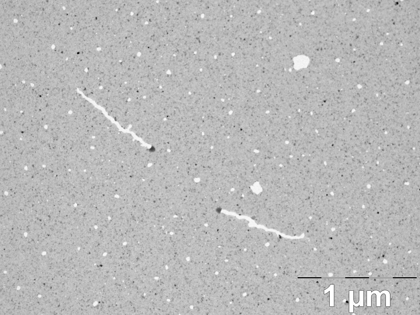 wafer 336 – 30kx
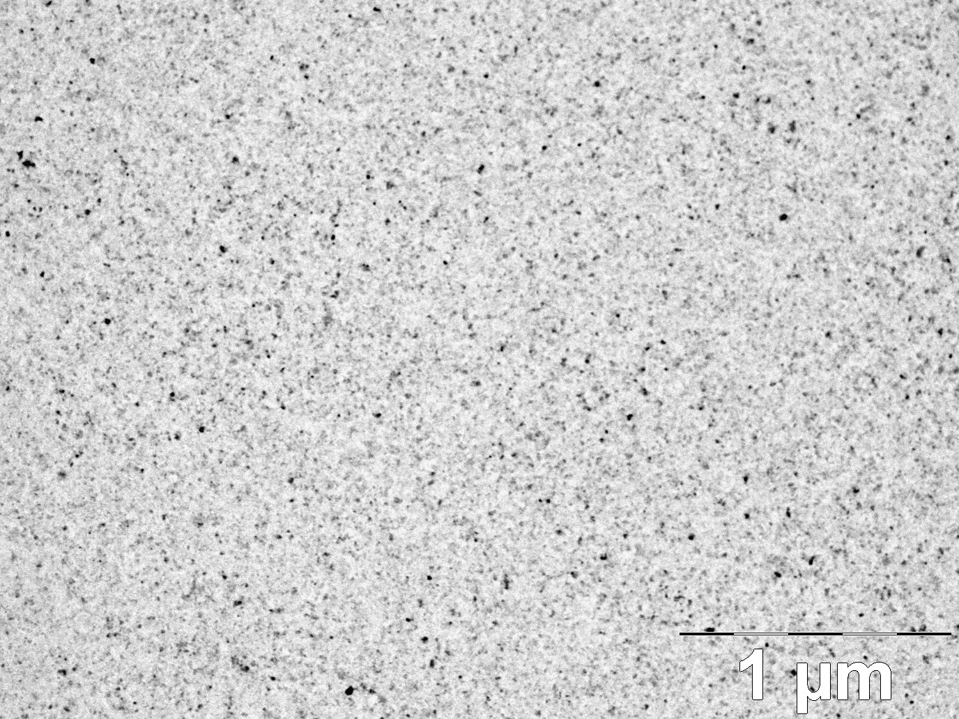 wafer 335 (0,0) – 30 kx – RT dep. + 950C RTP
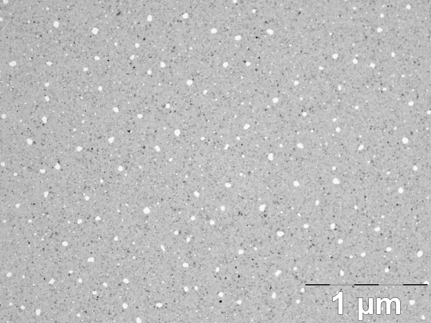 wafer 338 (0,0) – 30 kx – 400 C dep. + 950C RTP
Chris, JP, and I are discussing plans for a off-week in terms of production so we can focus on re-building the sputter heater. This will depend on how the wafers from this week look. We think the Cu is coming from a braze we used to attach the heating element to the SS plate. We’re brainstorming ideas on how to minimize the braze in the new design…