AFM of wafers
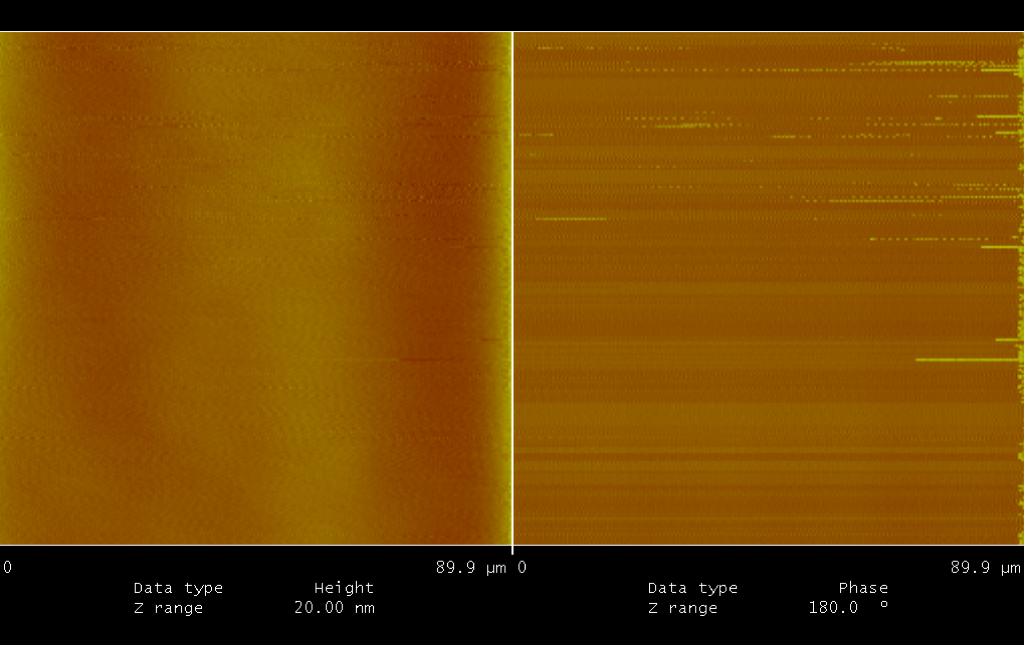
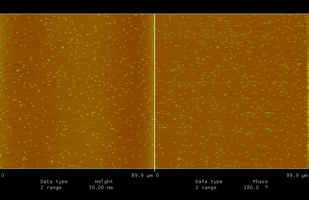
JP handed me a stack of wafers today, and I went over to the Krauss Lab and with the help of Jack Calcines got some AFM images. I didn’t have much time to play with, so I tried to get the most data I could quickly. I think we’ll have to do a more exhaustive study on our own (and hopefully on Waugh’s AFM once we get cleared to use it). For the images, the left panel is the z topography and the right is the phase.
First we looked at the 200um wafer. We took a couple images and found 1 large particle in one image and 2 in the other. The surface RMS was around .3nm omitting the particles.
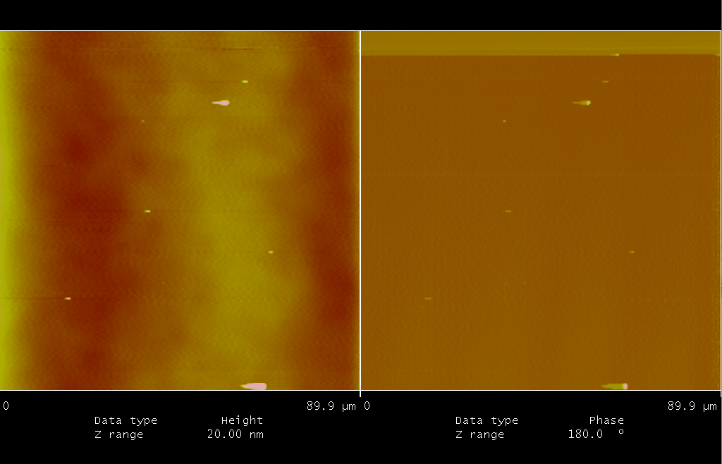
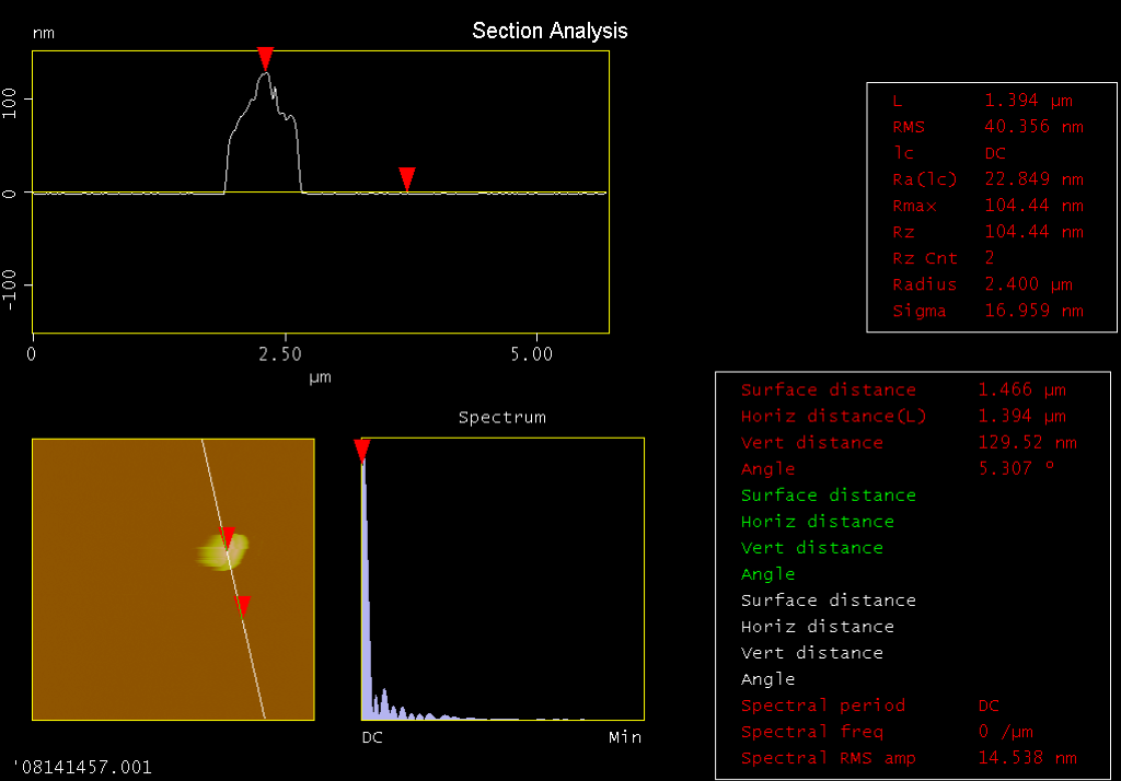
Center particle zoom in:
So we then looked at the 400um wafer and again took images in two different spots. The 400um wafer had many noticable little particles on it, but no large ones like the previous wafer. The particles averaged about 8nm in height. The z range is indicated under the images.
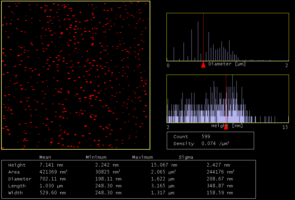
Here is some image processing for this image. The image is thresholded then the particle characteristics are measured and binned into histograms.
Chris recommended that we look at the 400um 2x SiO2 strip after the two factory wafers, and this was the last one I had time for. This wafer is completely clear of particles as compared to the factory 400um wafer. The roughness is also in a similar range with an RMS of about .4nm.