Membrane Edges with SEM
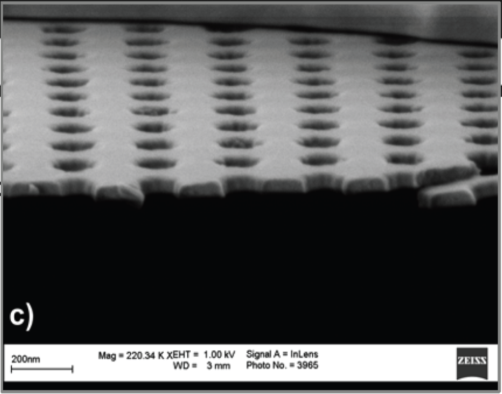
I was motivated to scan our membrane edges after looking at this image from the paper Maryna presented last week:
 I found a couple of pnc-Si samples with membranes still attached to the edges. I also found one sample with a membrane split almost down the middle. I coated the samples with 3nm of Au before scanning. I found that all of the broken membrane pieces were rolled up – there were few, if any, edges of membrane hanging into space.
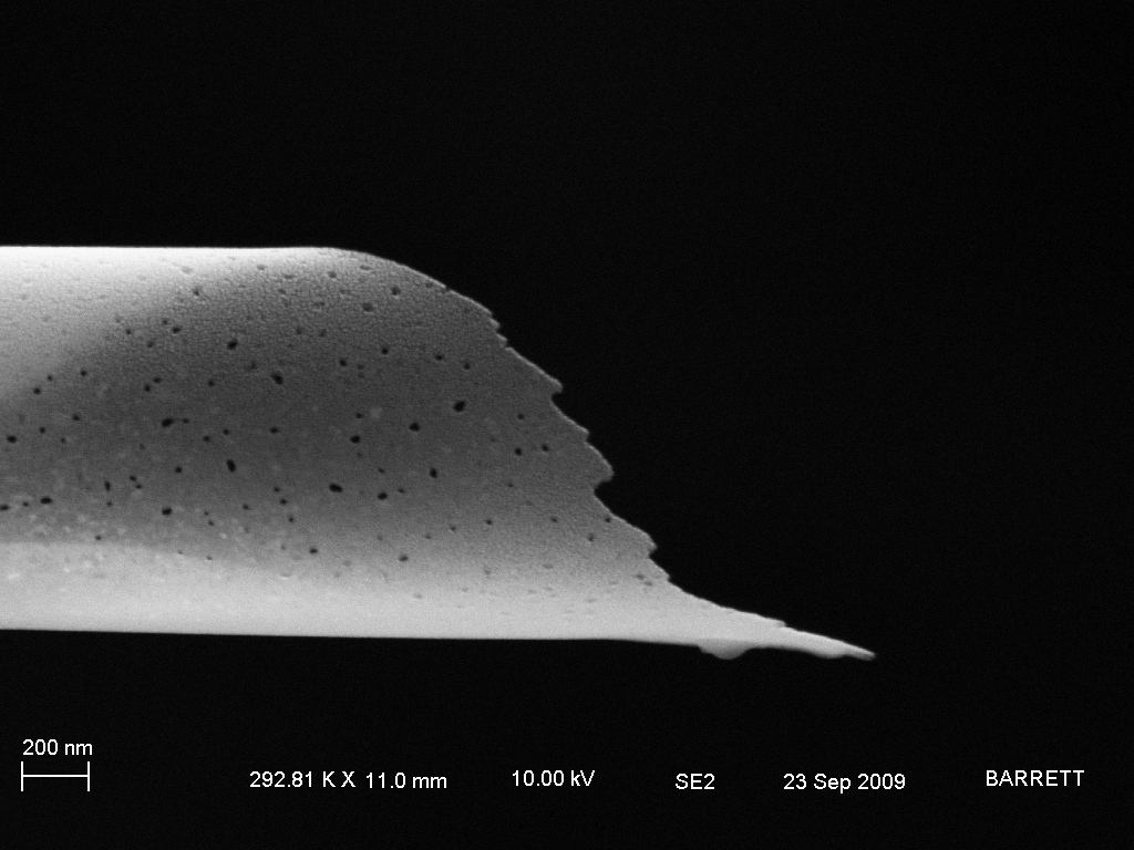
Here is a cigar shape membrane. The brighter, out of focus areas toward the left of the tube are area where the membrane is folded back toward the detector.
The edge didn’t come out very well on that scan, so I tried tilting the stage to align the detector with a broken membrane edge.
Instead I found another rolled up membrane, but here the edge is a more in focus.

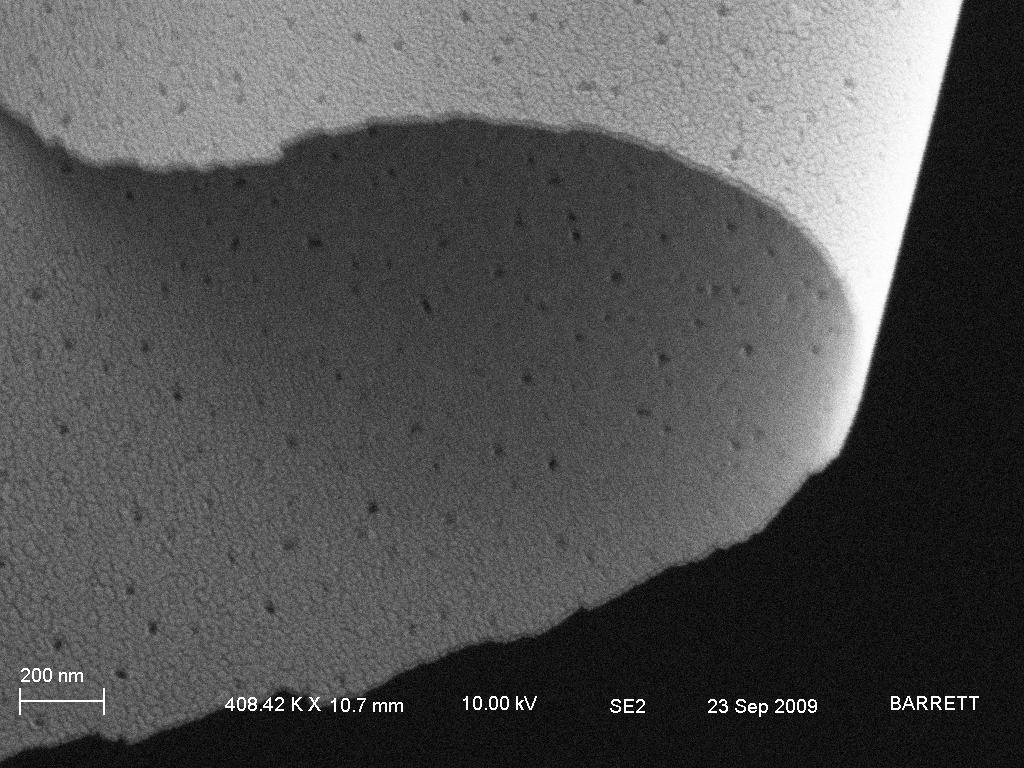
This is a higher magnification of an edge. The darker area to the left of the scan is membrane out of focus. The edge looks best in this scan. I could get this area into focus (I think) with a different aperture, although the electrons might deflect off the curved membrane area.
None of these scans looks as good as the one in the paper that membrane is 45nm thick with 120nm pores.. I think our 15nm thick membrane with slightly bigger pores is pushing the resolution limits of our SEM.
Beautiful! It almost looks like the membrane tears between the pores (like ripping on the dotted line). I can’t really tell the inner pore shapes too much from this though.
It also seems that our recent membranes have been a little thicker ~20 nm. Time for another re-calibration with the ellipsometer!
These look better than I would have guessed – I’m glad you took a look. They probably curled up because of the stress in the sputtered gold – if it was a problem, you could try without gold or figure out a way to put equal amounts of gold on each side. If you don’t coat it, though, it will probably charge and start bouncing around on you.
Given the unknown angle of the image, the resloution of the SEM, unknown calibration standard and date of the SEM calibration, plus the thickness of the gold layer, I’d believe that the silicon is pretty close to 15nm thick. Trust the ellipsometer!
Thanks to everyone for their comments and suggestions.
I’ve never been able to interrogate the inner pore geometry with the SEM – just been able to see that they are there.
I have no idea how often the SEM is calibrated. I wasn’t hoping to get a value for membrane thickness, I just wanted to look at the morphology of the edge.
During sputtering, I tried to tilt the samples to get Au on both sides of the broken membranes. It’s tough though because the samples don’t spin around during sputtering. Plus I didn’t want to risk breaking one of those delicate edges. One of the samples I looked at this week wasn’t coated and charging didn’t seem to be too much of an issue (although I was using lower kEv and mag for that sample). All of the unknowns you mention I can find out if we really need to know.