TEM on SiO2 coated membranes
As per Jim’s suggestion, I coated wafers 335 and 341 with 40.6nm SiO2 on top and 42nm SiO2 at backside. The membrane cells have been passed to Anant and Maryna for chemical stability and air flow tests.
Today I got some TEM images from the medical center with the help from Karen.
We first imaged wafer341 at 60k. There are a lot of white spots indicating pores on the sample. See Fig.(1) below.
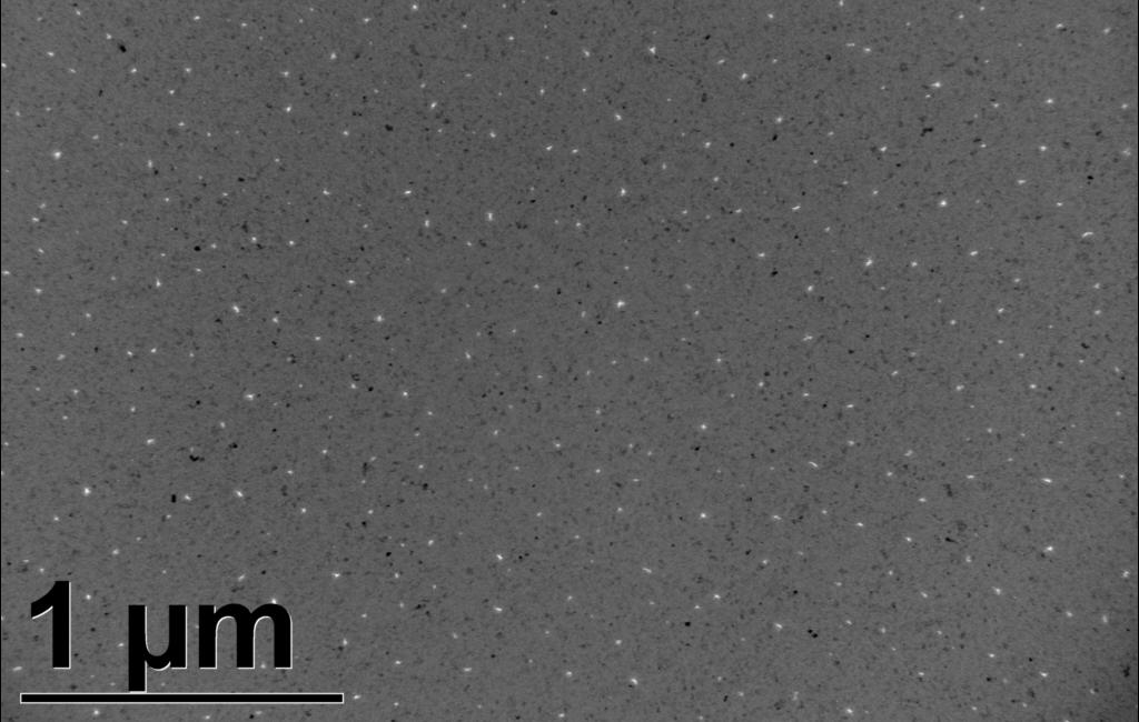
Fig.(1) wafer341 with 40.2nm SiO2 coating, imaged @60k

Fig.(2) wafer341 with 40.2nm SiO2 coating, imaged @180k
Then we switched to 180k, see Fig.(2). But at this high mag, i.e. high electron intensity, something interesting happened. Compare Fig.(3) and Fig.(4). The white spots indicating “pores”(not necessarily open though) became smaller and some of them finally disappeared after two minutes.
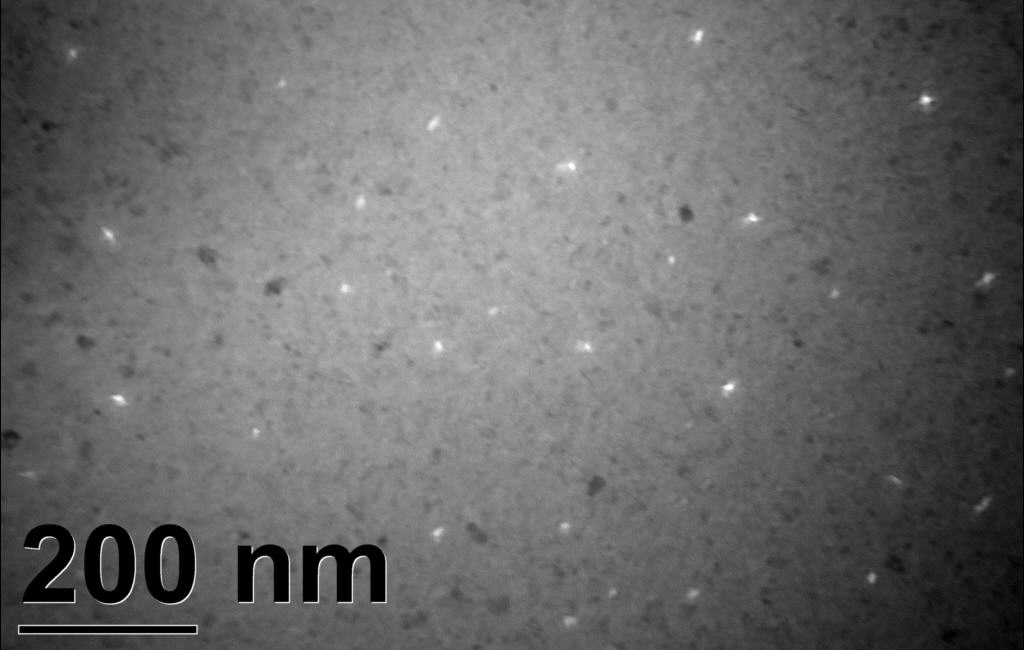
Fig.(3) wafer341 with 40.2nm SiO2 coating, imaged @180k, @ t=0
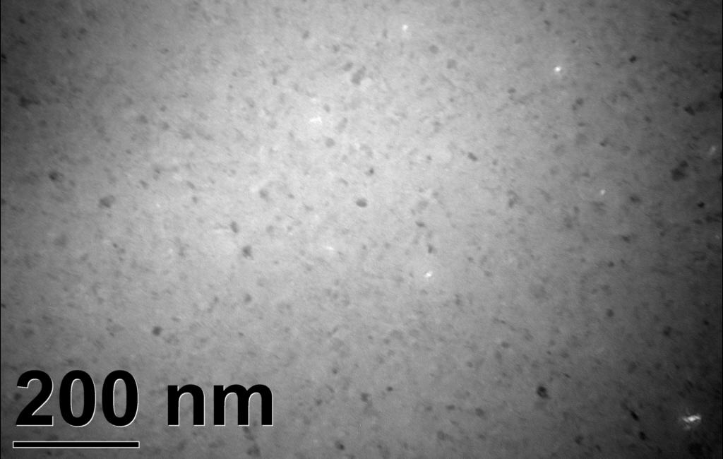
Fig.(4) wafer341 with 40.2nm SiO2 coating, imaged @180k, @ t=2 min
It looked like that this phenomenon only happens under high electron intensity (or high mag). In order to verify this, we switched back to 60k again. See Fig.(5),(6). There is almost no change after two minutes under low electron intensity (low mag).

Fig.(5) wafer341 with 40.2nm SiO2 coating, imaged @60k, @ t=0
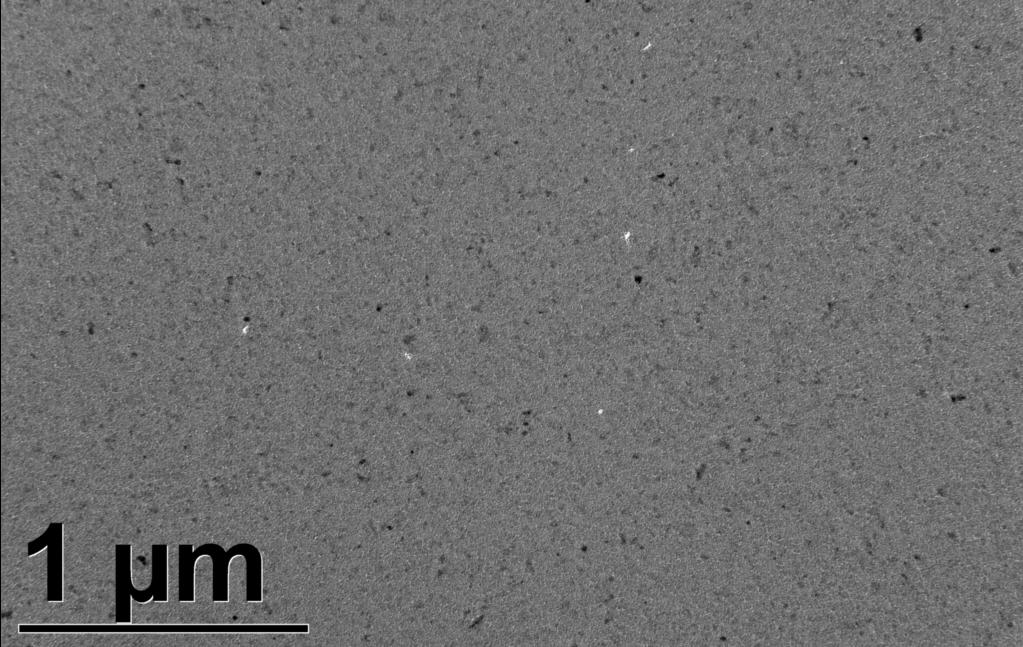
Fig.(6) wafer341 with 40.2nm SiO2 coating, imaged @60k, @ t=2 min
To explain this phenomenon, I guess it could be due to electron accumulation in the SiO2 layer. Since SiO2 is an insulator, under our processing condition, there could be a lot of electron traps
at the Si/SiO2 interface and inside the oxide layer. With more and more electrons trapped in the pore region, we lost electrons (may be due to repulsion) which could penetrate the sample at the “pore site” — hence a previous “pore” becomes “opaque”.
Above is only my hypotheses 🙂 We can discuss it in the group meeting.
For wafer335, there are less white spots on the coated samples. See Fig.(7) and (8). Probably because the porosity of this wafer is less than wafer 335. I checked the TEM database, wafer335 has smaller pores than wafer341. So most of the pores could be blocked by SiO2.
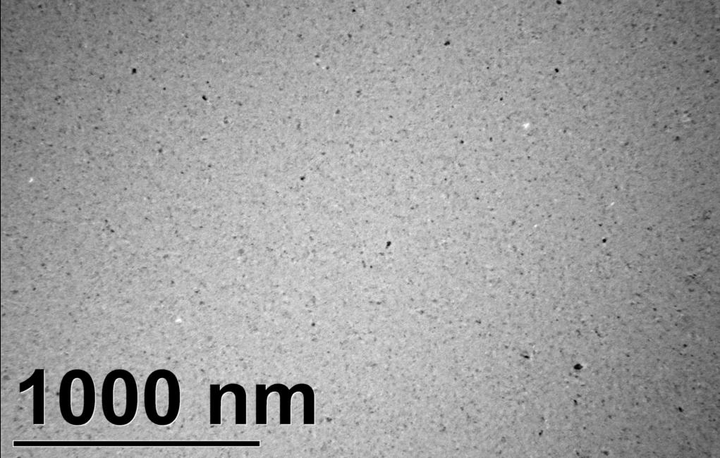
Fig.(7) wafer335 with 40.2nm SiO2 coating, imaged @60k

Fig.(8) wafer335 with 40.2nm SiO2 coating, imaged @120k
There is another unsolved issue. We are not quite sure if these white spots are open pores or not. But we suspect they are not completely open. The reason is that it is almost impossible to get a “sharp” image of these white spots, i.e. they are almost always out of focus. This could happen if some pores are covered/filled by a thin layer of SiO2. I think if we have Maryna’s air flow data, we can have more evidence.
Nice work and thanks for helping us do this quickly. I took a peek at Anant’s test and these appear stable too. Dave saw a similar phenomenon with pore shrinkage and reported on it in an earlier post.