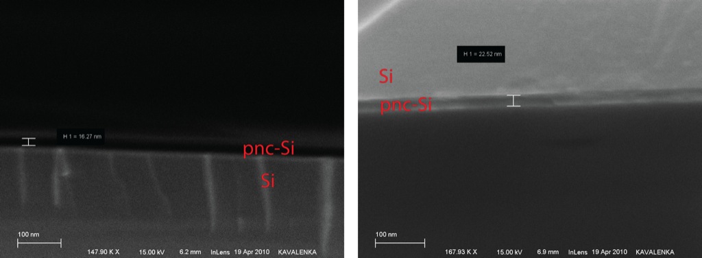
Measuring membrane thickness in SEM and updates
I tried to measure the thickness of the non-carbonized and carbonized membranes for the paper using SEM. To have a clear cut of the membrane I place the membrane chip upside down on a silicon wafer piece, then bend the membrane chip with tweezers so the membrane sticks to the wafer while breaking of the chip. It works well, before I used alcohol to de-attach the membrane, but this time didn’t want wrinkles and fracturing during drying. After the membrane is on the wafer, I cleaved the wafer perpendicular to the membrane strips to break the membrane along the cleaved edge. It is very hard to take this kind of image on the SEM as there are practically no features on the cleaved edge. The images me and Krishanu ended up taking are not very good, but give enough information to estimate non-carbonized thickness to average 23.5 nm and pnc-Si to 15.9 nm. The measured carbon ring thickness inside pores (TEM) is 2.5 nm, the carbon thickness on the front and back of the pnc-Si is approximately 3.8 nm (SEM).
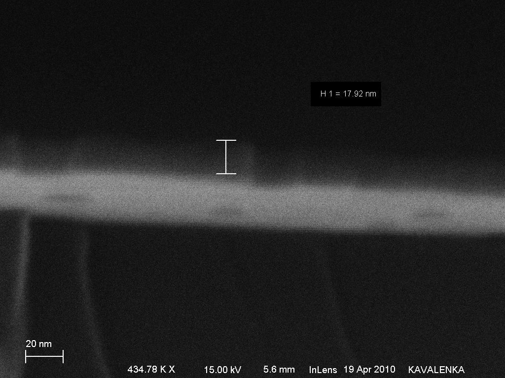
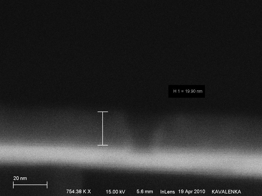
In the next two images the edge-broken conical pores on slightly tilted membrane can be recognized. All images are taken on wafer sc324:
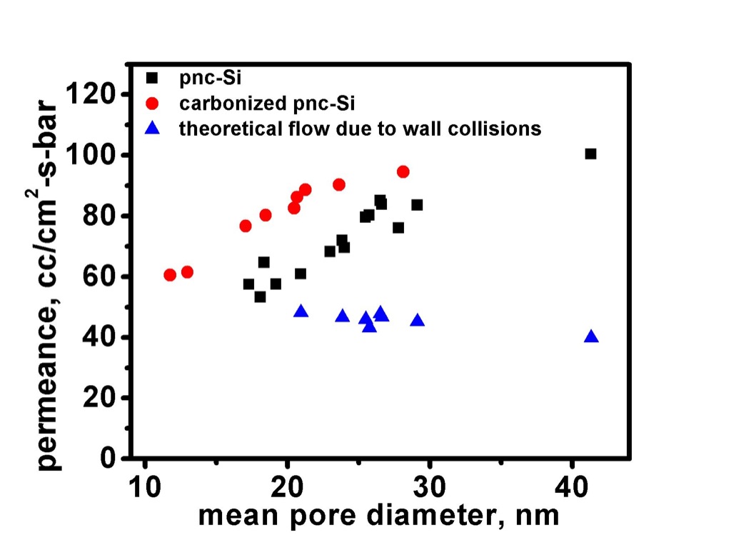
Ballistic paper updates to discuss:
1) The before and after carbonization data for few particular membranes is compared below on bar graph to predicted Knudsen flow through the same carbonized membrane (calculated form TEM):

2) The permeance values form the same wafers as carbonized membranes are added to the plot:
3) The equation mentioned before fix:
![]()