Pnc-Si cross section by FIB and cleaving
1) FIB.
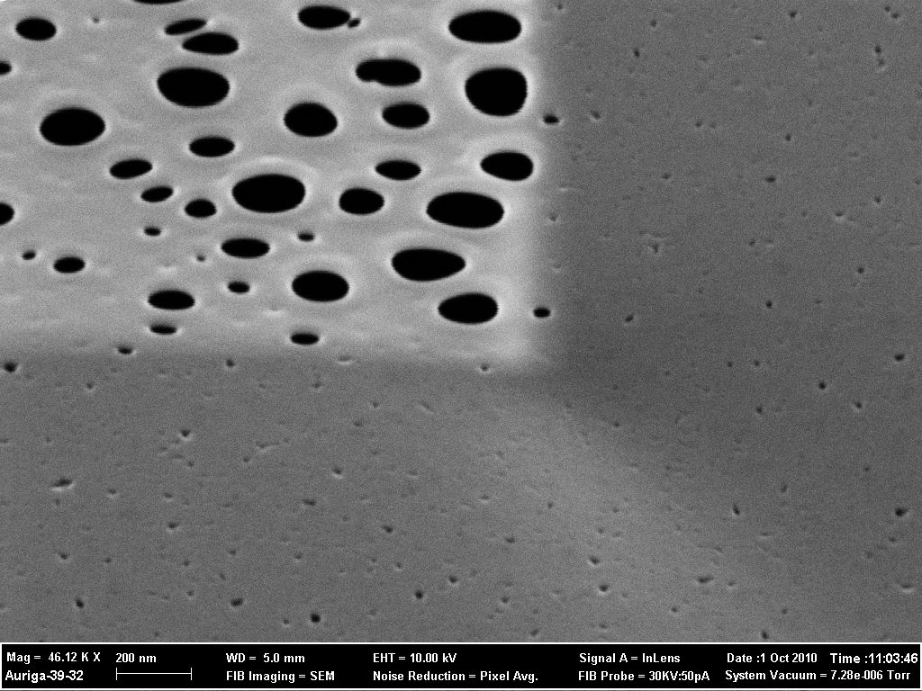
I tried to get a cross section of the pnc-Si with FIB with Brian’s help. The results are negative. It looks like the ion beam almost “melts” the membrane and destroys the pores instead of cutting. The tool also has in-built Pt deposition capability (from organo-Pt compound). So we tried to make the membrane thicker by depositing Pt, and then cut it. It also didn’t work. These are few interesting images from the cutting process.
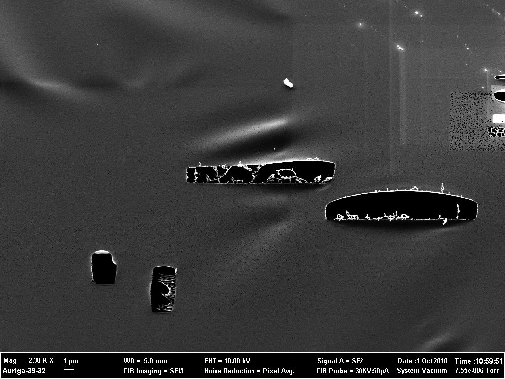
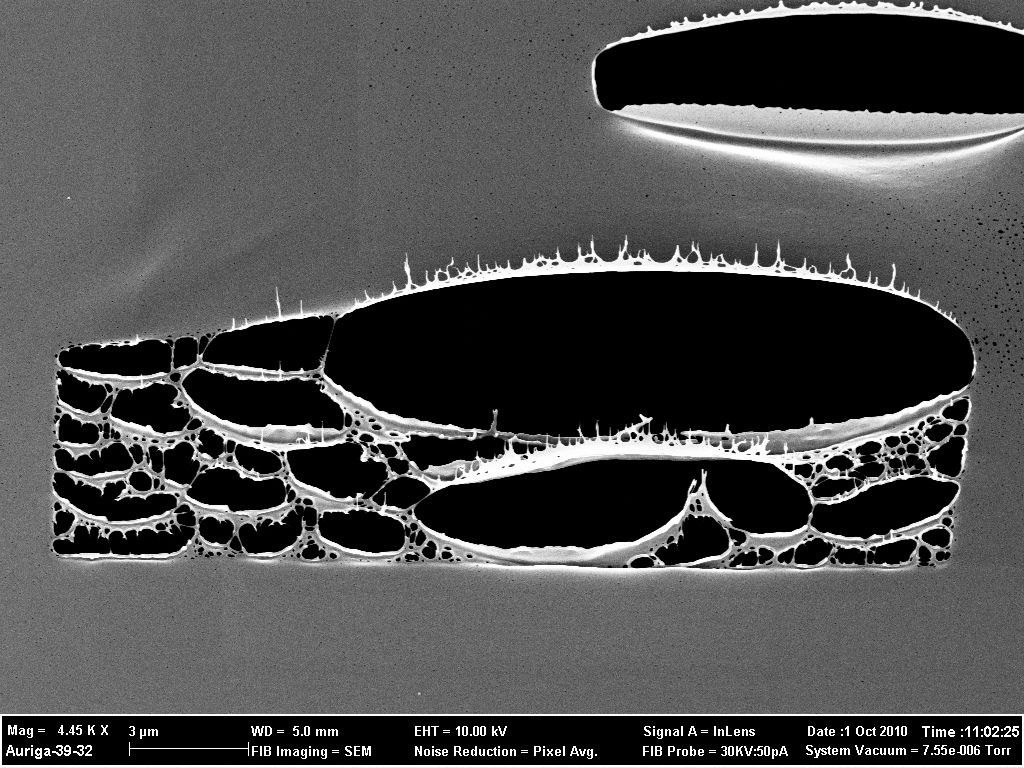
The pores expand under the ion beam:
During the whole process we made approximately 20 cuts of different shapes and sizes in the same area. The edges of the membrane in the cuts stretched and rolled, but membrane stayed perfectly intact
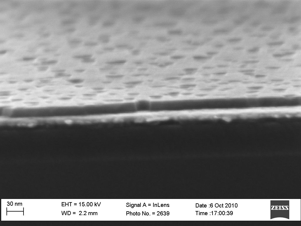
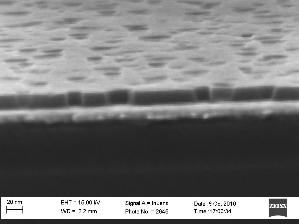
2) Cleaving.
I used this method before to take cross sectional images with Krishanu, but never got a good quality image. This time after trying different substrates for imaging, we took pretty nice images on the metallized wafer surface. We noticed, that pores in 15 nm thick membrane are mostly straight, and in 30 nm thick a lot of them are conical.
The two images below are taken on 15 nm pnc-Si. The metal layer below it is approximately 13 nm.