Metal deposition at different positions
I am trying to deposit metal on the membrane with minimal deposition inside the pores. The image below is an example of how the film quality and thickness change when the sample is positioned at different angles and distances from the source in the same deposition run. The schematic in the corner of each SEM image shows the sample position during deposition that yielded the film in the particular image.

Figure 1.
I looked on the cross sections of these membranes to see if the metal can be observed inside the pores. In all CS-SEM images the metallized membrane is on the bottom of the metallized pnc-Si substrate. By the way, the holes in the substrate in all cross sectional images are showing what happens to non-freestanding portion of the pnc-Si during BOE etch, when the bottom oxide is partially etched away.
(1) cross section of the 1st image in Figure 1 (metal deposited only on one side – top)
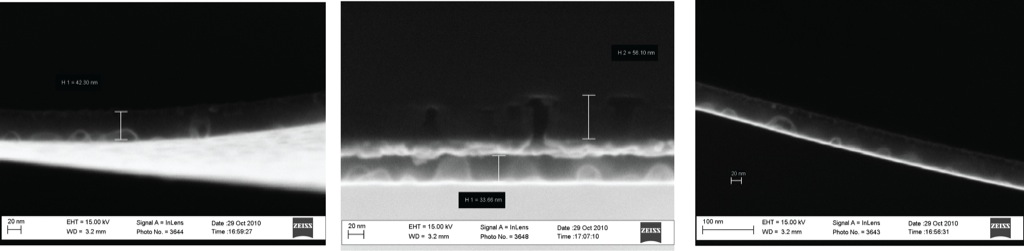
(2) cross section of the 3rd image in Figure 1 (metal deposited on both sides of the membrane)

The pores in (1) look much cleaner and have less debris than in (2), which probably means that less metal gets inside pores when the substrate is positioned at extreme angles during deposition.
I also made conductivity measurements on all three sample types in Figure 1. The samples of first two types have high (or infinite in 1st case) resistances, due to layers being not continuous, although not always. I am still trying to make sense of the data and will tell more on the meeting before writing about it.