Update: 30/100/30 OSO, 30/75/30 & 30/100/30 NSN SEPCON
We are trying to reproduce the very small pores Joe created with 30/100/30 OSO and large pores created with 30/100/30 NSN using a SEPCON pattern. (Joe’s previous post.)
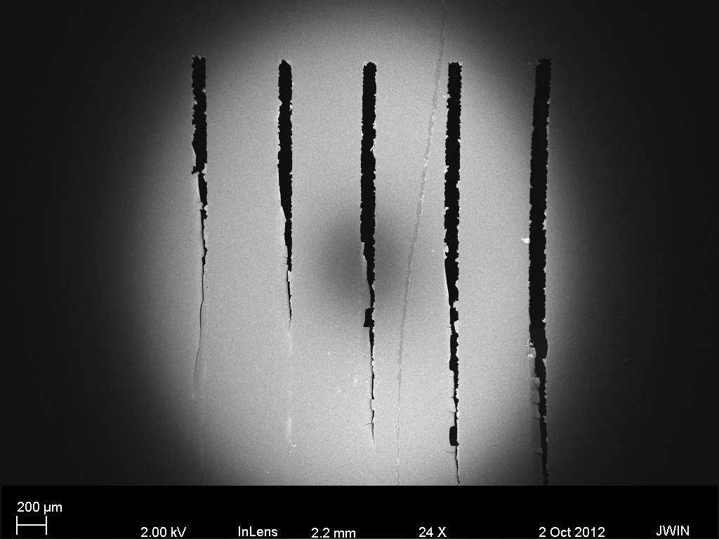
We had a problem with several chips releasing from the center of the wafer prior to completely clearing all the features. In the future we will use a different mask with smaller trenches to avoid this problem.
All samples were annealed in the RTP at 1000C for 1min with a 50 C/s ramp rate in the susceptor.
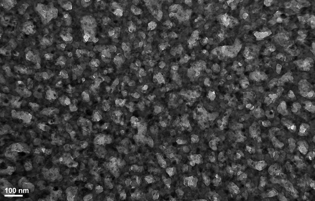
The 30/100/30 OSO wafer had ~ 50% of the SEPCON chips completely survive the process. Here is a typical TEM image:
The 30/75/30 NSN wafer seemed to delaminate during RTP. Half of the front surface of the wafer looked “ashen” after the RTP. The rest of the wafer, while with a better color, did not have any completely surviving chips. We did not have any surviving TEM grids from the wafers with NSN, so the following are SEM images of 30/75/30:
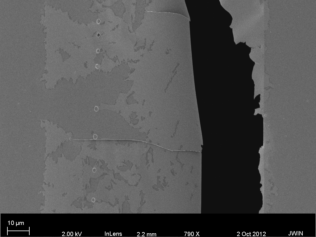


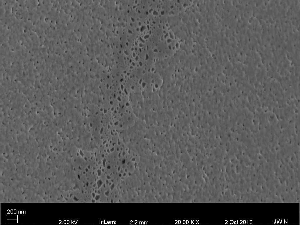
And next are 30/100/30 NSN. This wafer did not delaminate during RTP. Even so, only a dozen chips completely survived. It looks like large pits, but small pores:

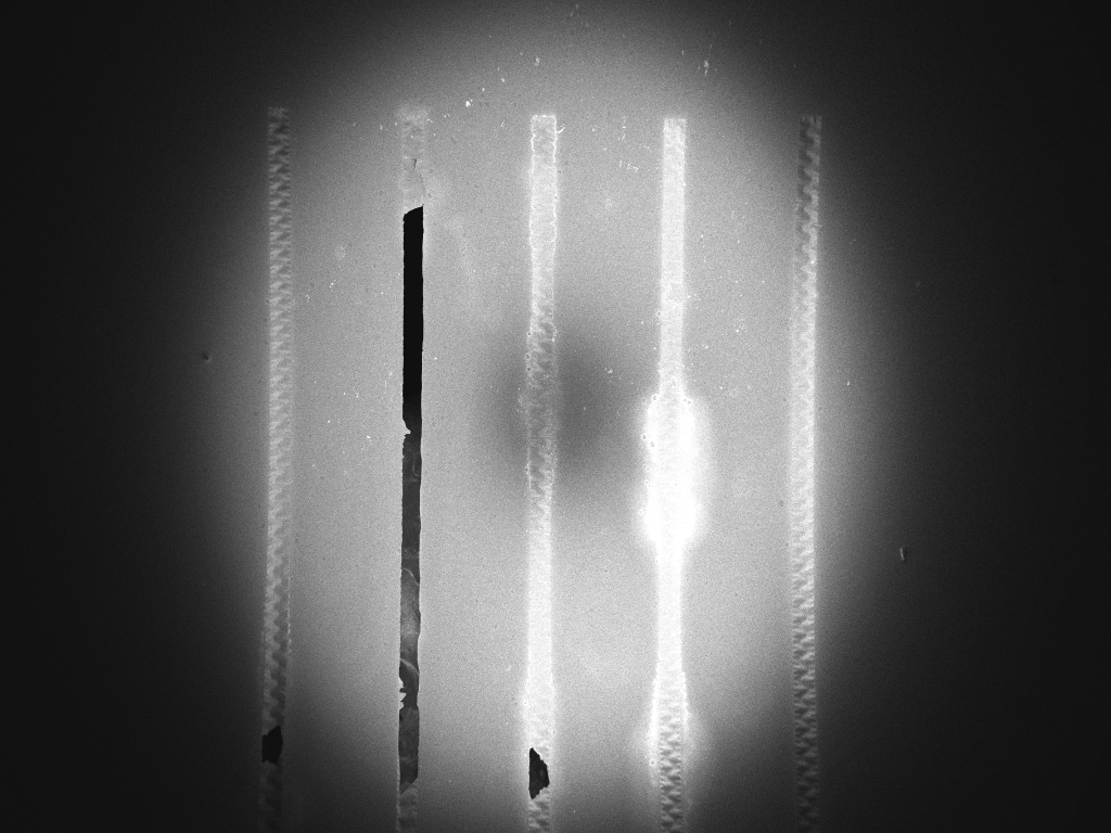
Charles got a section of the membrane onto a separate TEM grid and got an image verifying the unexpected smaller pore size:


The OSO stack looks very similar to my previous result, however the NSN stacks you made look quite bizarre. Despite etch first or anneal first, pores should be able to be observed from the SEM no matter from the free-standing membrane area or silicon layer on the substrate. I guess you have to redo the NSN stack. Use SimPore’s etch cell at RIT for the etching if possible.
Did you trip the nitride films? Was the etching clear? It looks to me that there’s something on your silicon layer that may cover the real features.
The nitride was stripped with a ~4.5 min 50% HF bath. As I said above, Charles laid the pnc-Si from the SEPCON on top of a 5nm nitride TEM window. Maybe the nitride is “blurring” the image slightly.
My advice would be to NEVER etch at UR again. Please work with JP at RIT, since this is really a standard process now and there is no reason to have this complicating experiments. SiMPore rents a bench at RIT strictly for etching, so everything is optimized, and this is a resource that should be used as much as possible.
Regarding the different looking material, this must be a process difference. Josh and Joe should talk by PHONE or in-person, and they should go over Joe’s process in excruciating detail to figure out where the disconnect is. An assumption is being made somewhere and we just need to figure out where. That being said, the lifting off of the Si film is the ultimate end-point of our pore formation process, effectively reaching 100% porosity. I would say that one of the steps in Josh’s process is too aggressive – perhaps the RTP – susceptor vs. no susceptor? SiN type and deposition conditions?
All the issues here seem fairly simple and I’m confident we’ll have good looking material shortly. I’m generally available to meet on campus or talk by phone, if I can be of any direct help. Thanks!
Chris, As we discussed briefly, I don’t think the problem is with the etch cell. Joe used the same cell to get his results. I believe the problem was that the trenches in the pattern that I used were too large. Maybe the other etch cells would have been “gentler” during the etch and we could have avoided the chips lifting out before total completion. I am hoping that using the standard mask for SEPCONs that JP uses we won’t have this problem because the trench size should be slightly smaller. We are hoping to process the wafers as much as possible at URnano and if we can continue to etch there that will simplify things. That said, if there are any problems with the next wafer using the typical pattern in this etch cell I will be more than inclined to use the RIT etch cells.
I will call Joe tomorrow and grill him for info.
I also have ~10 SEPCON chips with 30/100/30 NSN that have not been RTPed or stripped because they have broken windows. I will try annealing some with varying conditions and investigating with SEM while I wait for the AJA to free up.