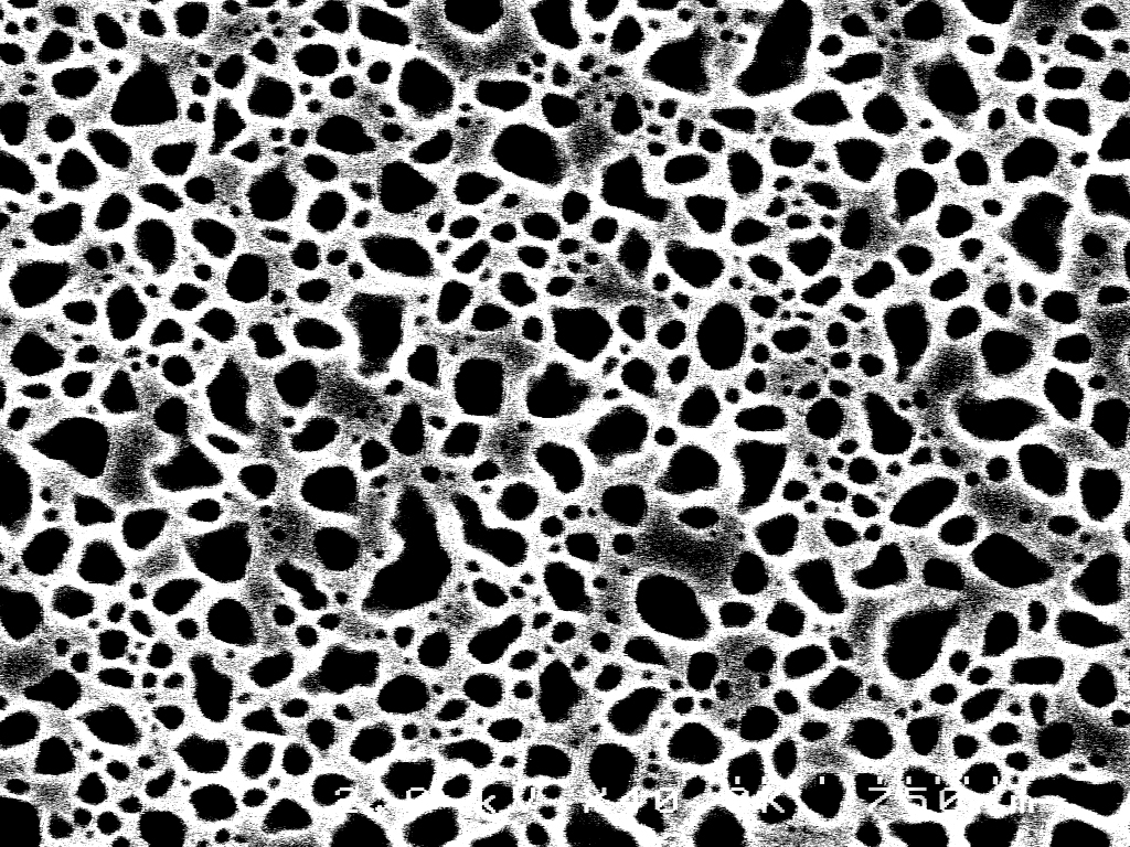
NSN stacks with different Si thicknesses
In this post, I sum up all the NSN stacks with different Si thicknesses I have made so far. The nitride layer is 30nm thick for both the top and the bottom. The thickness for silicon film ranges from 7nm to 10nm, 15nm, 25nm, 50nm and 100nm. All the wafers were firstly etched and then annealed. The annealing temperature is 1000C for 1 minute with a 50C/s ramp rate. The following is the TEM images of annealed NSN stacks.

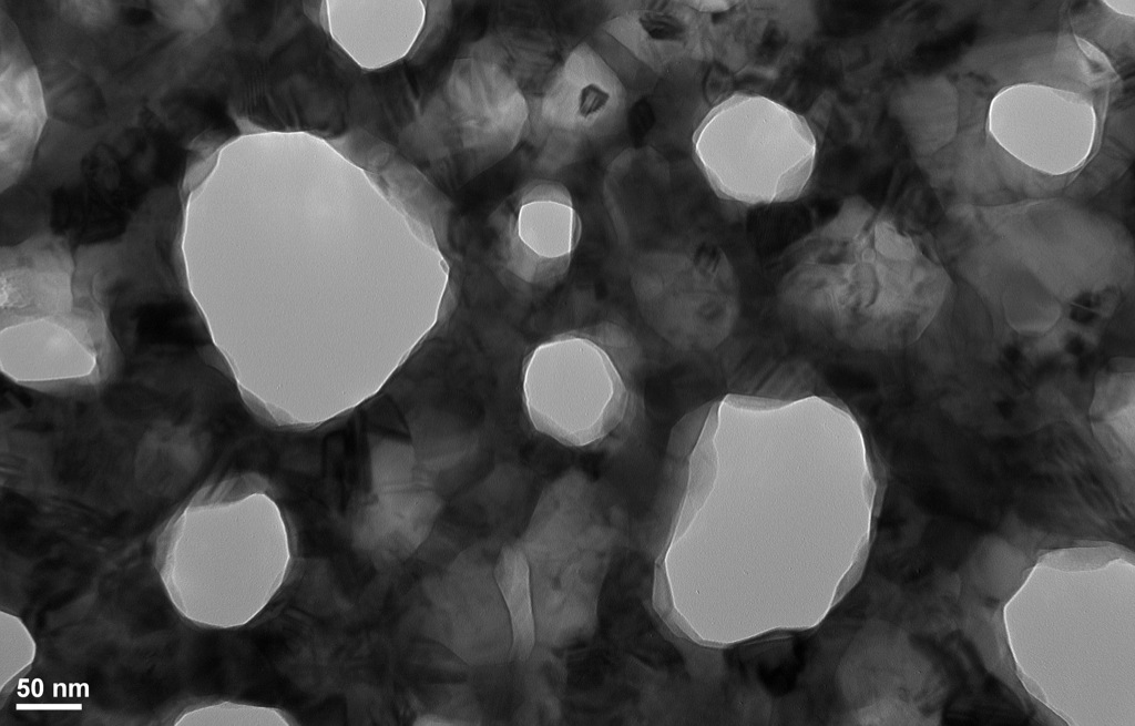
The image a, b, c, d, e, f represents NSN stacks with 7nm, 10nm, 15nm, 25nm, 50nm, and 100nm, respectively. Surprisingly, nanopores are observed in silicon layer even it is only 7nm thick, which is not gonna happen in OSO stack. Both the size of nanopores and silicon nanocrystals grow with the silicon film thickness. The next few plots are pore characteristics plots including porosity, pore density and average pore diameter.
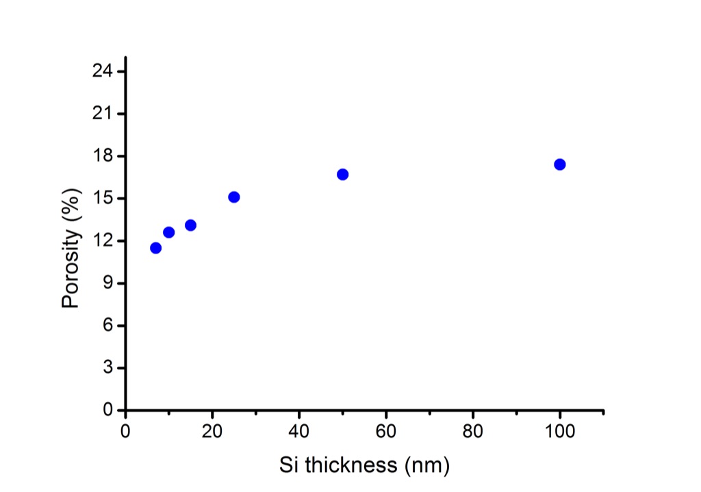
From the porosity plot, it can be seen that the porosity increases with the silicon thickness and it seems that it starts to saturate at around 18% when the thickness of silicon layer reaches around 50nm. The porosity for the 7nm thick Si layer is around 11%.

The next plot is the average pore diameter plot. It shows that the average pore diameter also increase with the silicon thickness and the increase rate becomes bigger when the silicon layer goes thicker than 25nm. One thing needs to be pointed out is that the average pore diameter ranges from around 17nm to about 100nm when the silicon layer goes from 7nm to 100nm. This is a broader range than the OSO system and it indicates that we are able to tune the pore size in a larger scale than we used to.
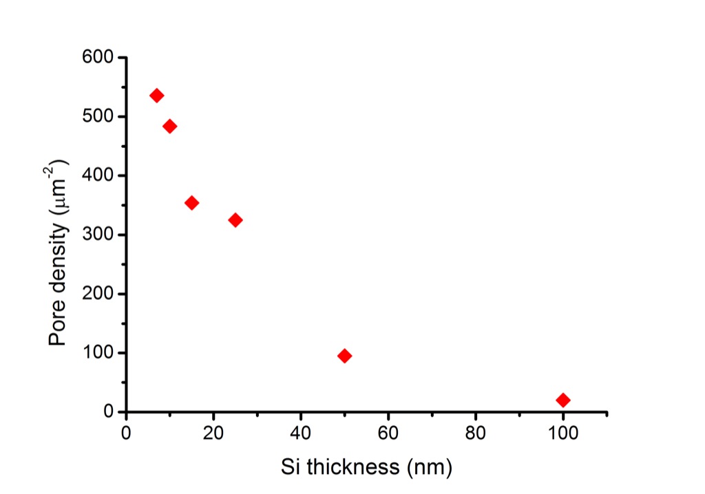
The last plot is the pore density plot. It is not surprising that the pore density decreases with the silicon thickness since it becomes harder to form a open pores in a thicker film. The density of nanopores from 100nm thick silicon layer becomes very low. However the reason for the high porosity from the 100nm thick silicon stack is due to the largest pores that formed in silicon layer.
In sum, NSN stack offers a very broader way to tune the pore size and porosity than the OSO stack. Nanopores are able to form in silicon film from the NSN system even the silicon layer can be either very thin or very thick. This ability makes the NSN stack to be the best candidate for the separations.
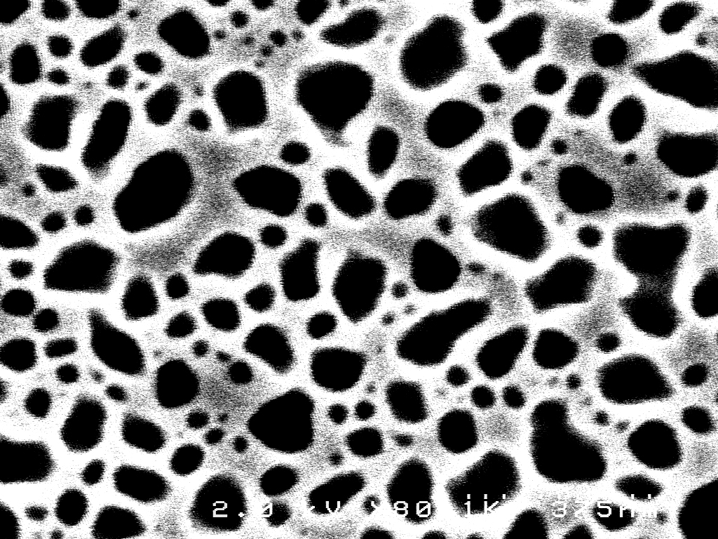
Here are some TEM images of annealed 100nm thick NSN stack with different magnifications.


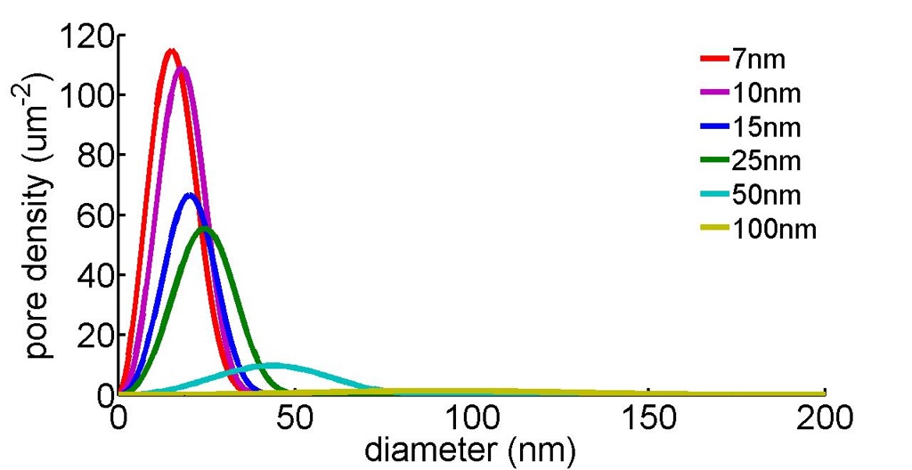
Here are some additional plots. The first one is the pore distribution plot of all NSN membranes.
The next one is the pore distribution plot only from NSN stack with 100nm thick Si layer. Note, this plot is from a TEM image at 50K magnification.

The last two images are SEM images of 100nm thick NSN stack. The images were taken from Vanderbilt University using a Hitachi S4200.
On the porosity plot, the value near 20% for the 100nm film does not agree with image F, where the porosity is <10% by my calculations. Was a different image used to calculate the porosity? If image F is not representative of the material because the pores are so large, please add a lower resolution image to the post so we can better understand the film.
Also, are the yields that you get on these membranes fairly good or are some of them difficult to make without cracks or defects? With our application focus, we may get requests for 100 dialysis chips for any of the membranes that are shown, so it would be helpful to understand if they can be easily made.
Thanks!
Also – sorry if you have posted these answers in the past, but:
Do you use a susceptor or not during the anneal?
How long does it take to sputter the 30nm of SiN on both sides?
How long does it take to remove this much SiN and what solution do you use?
Thanks!
To your questions.
The average porosity I calculated for 100nm NSN stack is around 18%. I cropped the TEM image with a square size and that’s why it looks less porous . I upload some images with different magnifications. The result should be very close.
I first etched the wafer and then annealed some popped-out grids within the susceptor, so I don’t know the yield. From my past tests, I haven’t seen any film cracks on the TEM grids. I didn’t check the pine hole on my wafer.
It took around 20mins to deposit 30nm SiN from my last run. I use pure HF to trip the SiN and I don’t have an accurate etching rate. The way I did it was that I sacrificed one grid in HF solution to see how long would it take to lift off my film and the actually stripping time is slightly below that lift off time.
One thing I did notice is that the film is not flat after stripping the nitride. And it seems same to most NSN stacks regardless of the Si thickness.
Discussion at NRG: Lets look at histograms. We think the ‘missing porosity’ might be internal pores that we can’t see by TEM. Tom suggests that the histograms should become more narrow for the thicker material.
Can you check?