E-beam Deposition of Ag, Cold ALD Runs, and Sepcon Assembly For Making a Nanofluidic Transistor
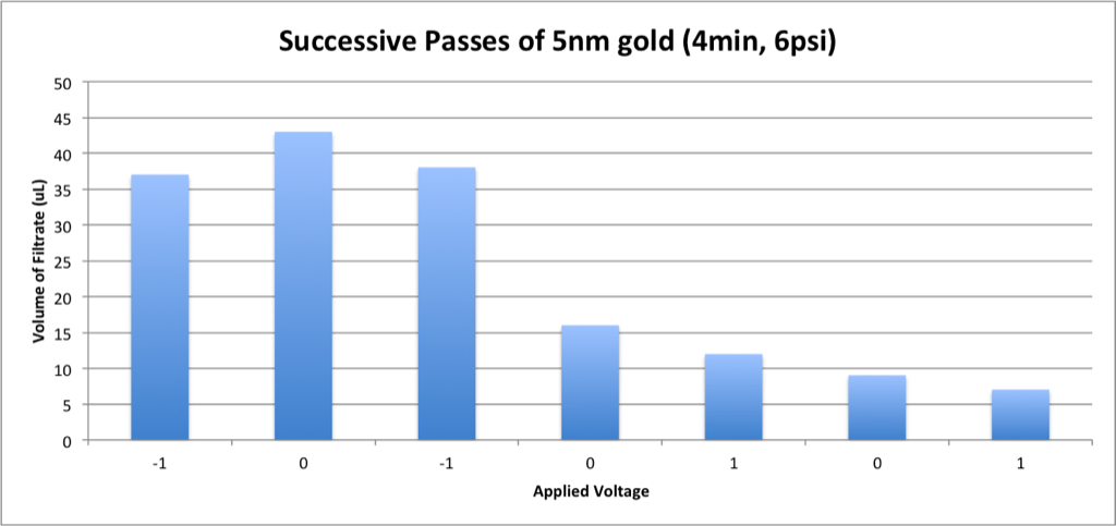
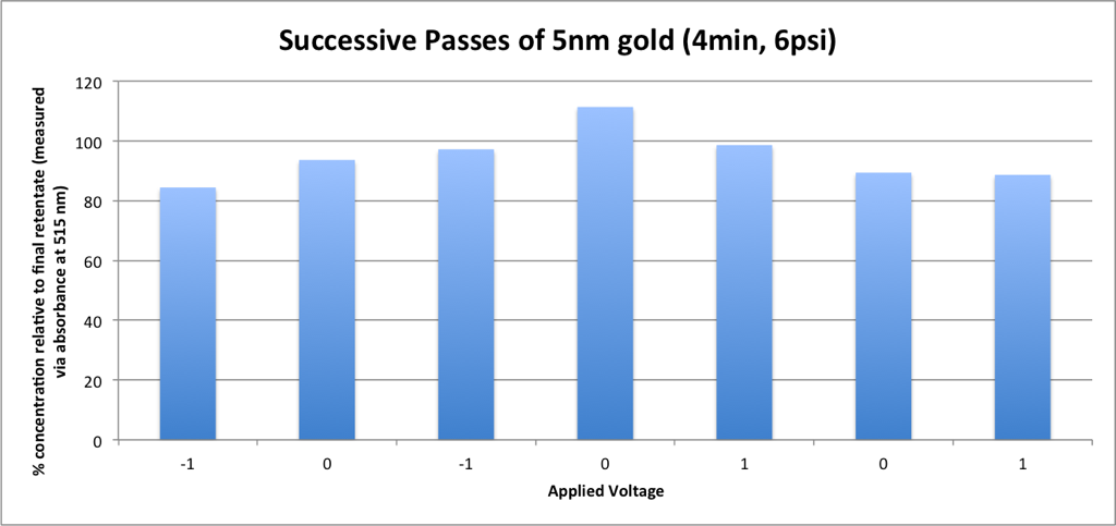
Last week I conducted a variety of experiments to try to make a nanofluidic transistor (a device described in detail in this previous journal club post). I did some light optimization of the E-beam deposition of Ag films over a 3nm Ti adhesion layer in the PVD lesker machine and found that 12nm of Ag gives an unbroken film of silver that reduces the resistivity of the silicon wafer from the megaohm range to the ohm range. I used Krishanu’s recipe for 100C depositions of Al2O3 in the ALD, and I used a piece of copper foil to attach a function generator to the conductive part of the membrane while the membrane was inside the Sepcon housing. A series of passes of water seemed to show that -1V applied to the membrane increased the hydraulic permeability of the membrane by ~25%. Unfortunately, adding 5 nm gold nanoparticles gave me some inconclusive results – the concentration of gold in the filtrate was constant regardless of applied voltage, and hydraulic permeability seemed to to decrease when -1V was applied.
Krishanu found in this previous post that 12 nm of Au over a 3 nm Ti adhesion layer was sufficient for a quality film. He also found that keeping the chips on the outer rim of the platen gave a more uniform film. Because of the expense of using gold, I’ve switched over to Ag. I did a series of depositions on some TEM grids:
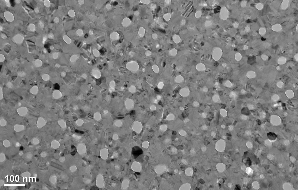
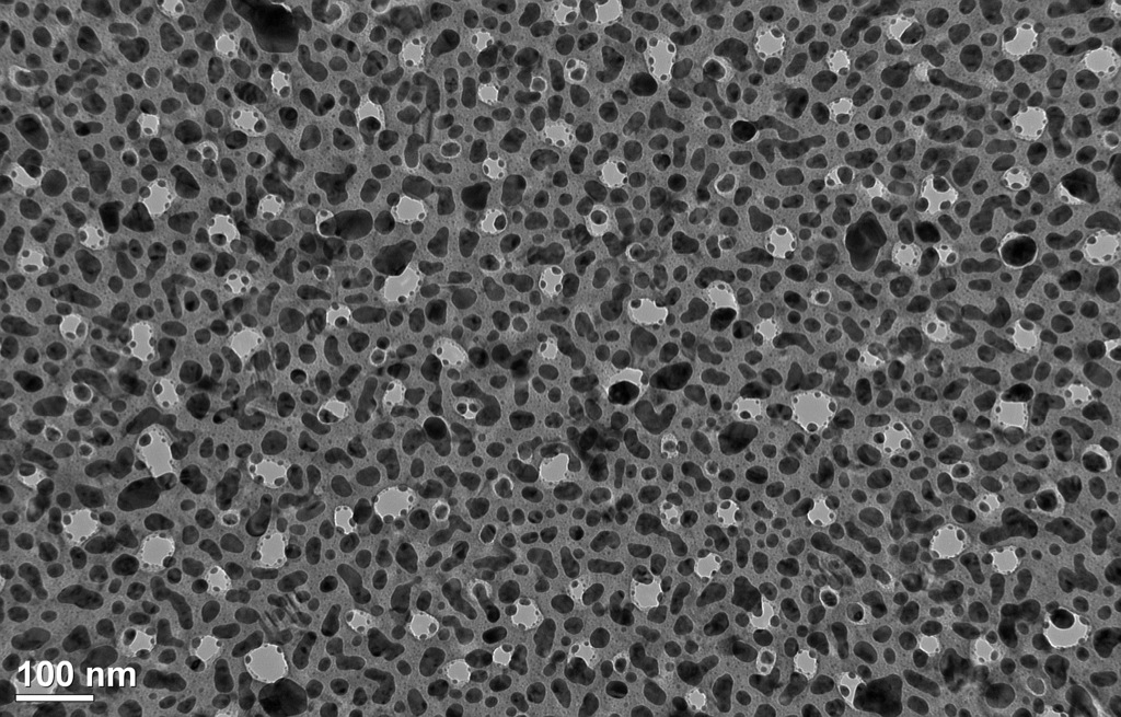
Bare TEM grid:
4.4 nm Ti, 4 nm Ag, Center of platen:
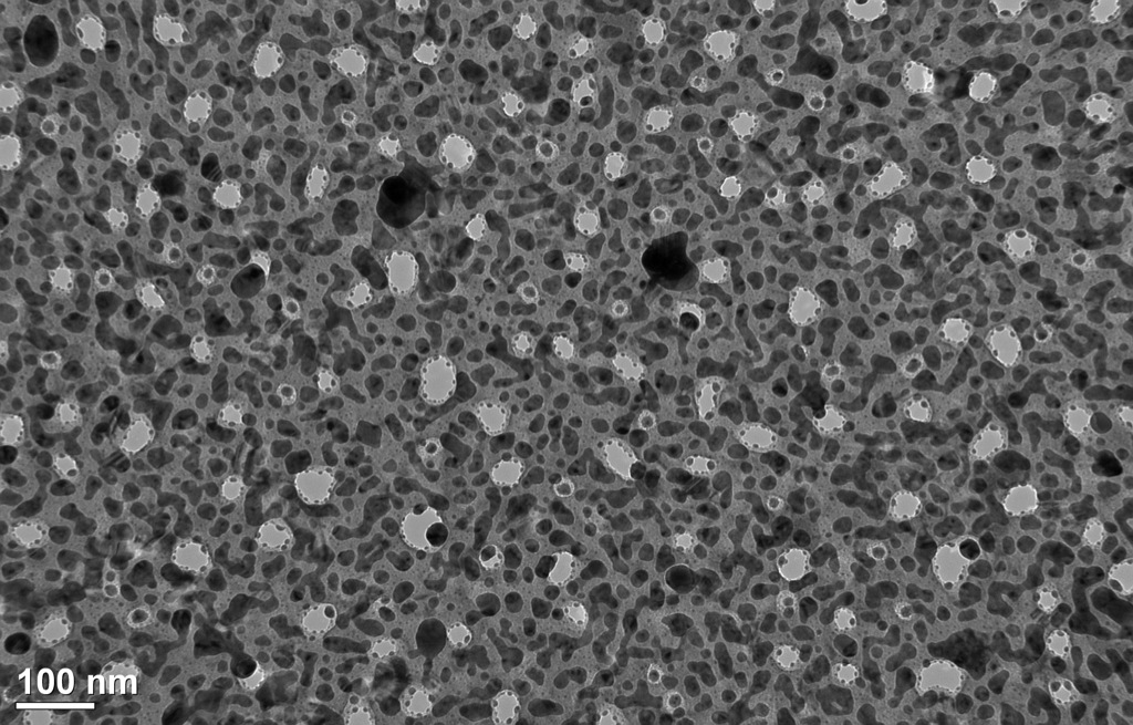
4.4 nm Ti, 4 nm Ag, Edge of platen:
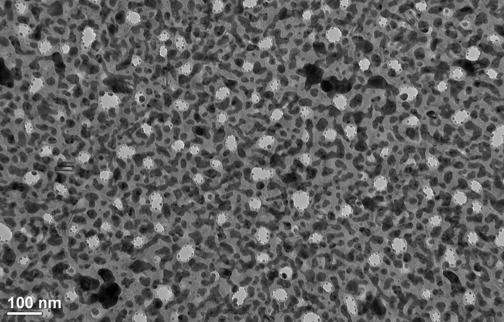
3.3 nm Ti, 4.9 nm Ag, Center of platen:
3.3 nm Ti, 4.9 nm Ag, Edge of platen:
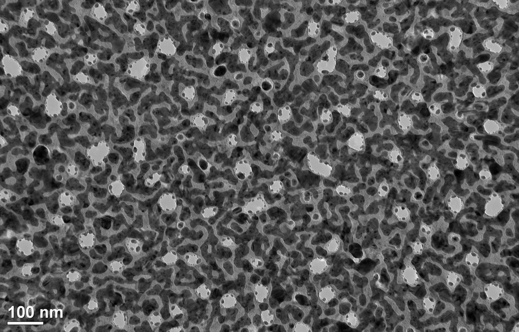
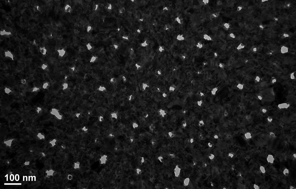
3.3 nm Ti, 12.3 nm Ag, Center of Platen (this chip broke when I removed it from the Kapton tape)
3.3 nm Ti, 12.3 nm Ag, Edge of Platen:

3.5 nm Ti, 25 nm Ag, Center of Platen:
3.5 nm Ti, 25 nm Ag, Edge of Platen:
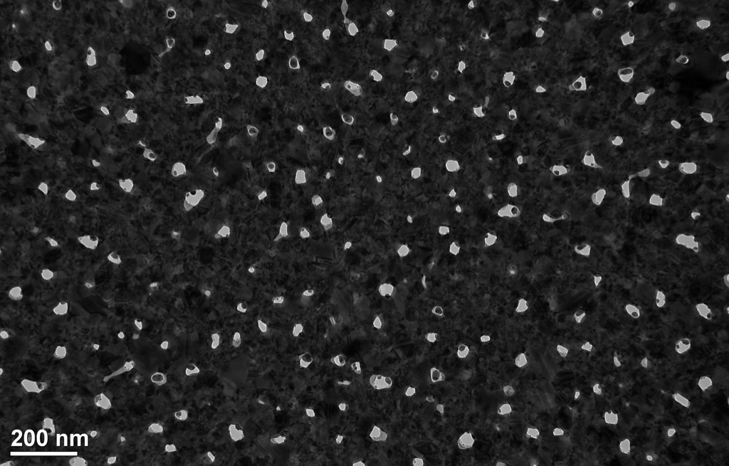
Of course the one we cared most about (12 nm Ag, Center of Platen) broke. But looking at these images, it seems clear that 12 nm Ag is a good thickness, and at the center of the platen we seem to get less holes totally filled. For the remainder of this post, I used these conditions.
Next, I took advantage of some of the work that Josh has done to try to make the ALD less of a violent machine (in my previous post my chips were getting buffeted by some pretty high pressures in the chamber. I believe Josh just lowered the input pressure of the driving N2 feed from 80psi to 40psi. It’s still not perfect:
(Tom said they used to be able to set chips at an angle, like so, without them moving), but at least the chips aren’t being flipped and shot about.
I used the following recipe:

From Krishanu’s email: “The recipe you want is Al2O3_100C_Beams or something similar. You need to set the substrate heaters to 100C and the Manifold, Valve and Trap to 150C like normal. According to Ryan, it deposits at the same rate as the 250C process (1.1A per cycle). *Note, heater 10 should be 100C, not 150)”
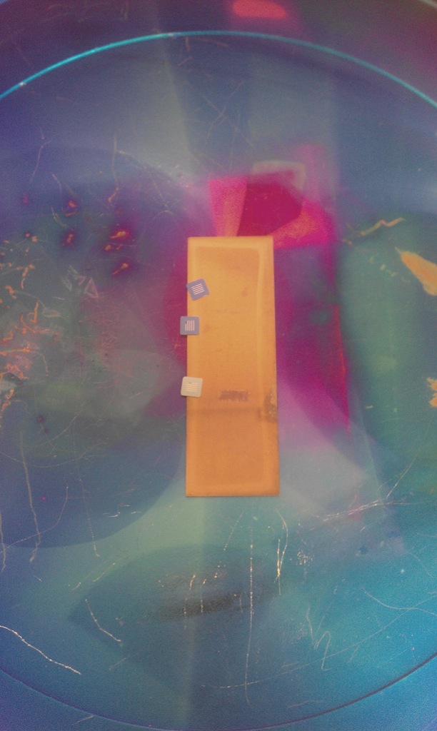
I deposited 5 nm of Al2O3 on 4 of the chips, and 10 nm on 4 more. I used Kapton tape so that at least one small square of silver would be left exposed for attaching a lead to:

I took some resistance measurements using a voltmeter in the cleanroom, but I had trouble getting consistant measurements. Typical resistivity of bare silicon was in the megaohm range, 12 nm Ag films were roughly 30 ohms (although this varied quite a bit as my hands shook) and both 5 and 10 nm of Al2O3 overtop of the silver failed to increase the resistance, probably because I was punching through the alumina with the leads (thanks Josh for the heads up). I suspected at the time that 10 nm Al2O3 wouldn’t be enough to insulate the silver, but in the paper linked above they were able to get an insulating layer with only 10 nm.
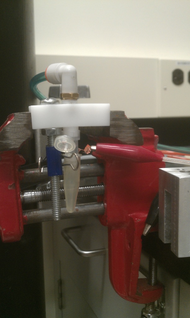
Next, I used copper foil and the sepcon housing to attach a function generator to one of the membranes with 10nm Al2O3:


I then did a series of water separations, alternating between no applied voltage and -1V:
After this apparent success, I removed the water and did the same thing with 5 nm gold, and then I applied alternating voltages of +1V and 0V just for the sake of collecting more data:
I’m not quite sure what to make of this data, especially since the absorbance at 515 for each of the filtrates (absorbance peak of gold) followed its own mad logic:
Future improvements:
Use silver epoxy instead of conductive copper tape for attaching the lead to the membrane
Verify that the function generator is giving us a constant -1V signal using a voltmeter.
Verify that current isn’t leaking into the solution by probing the fluid in the Sepcon with a voltmeter.
Find a way to verify that the silver epoxy is indeed in contact with the Ag film.
Neat!
When we discussed the ALD, I pointed out that the manual suggests 20 psi. 40 psi is what someone in the clean room has chosen. There may or may not be a good reason to use 40 psi instead of 20 psi.
Alex also suggested manually closing the valve for the nitrogen and slowly opening it after giving the vent command, this way you can ensure a slow vent.
It looks like using kapton tape as a mask worked well for you, but I would be a little nervous that the tape could peel off your deposited metal, or leave behind a residue from the adhesive. Just something to keep in mind if you ever have problems with that contact.
Looks like real progress on the membrane fab.
I don’t know what to expect with the water and particle studies. So the transistor works because of the competition between Electrophoresis and EO. EO happens toward the anode. I’m assuming that the anode is in the filtrate side. So shouldn’t this slow down flow? You are using DI water? Do we have any experience with EO and DI water for pnc-Si? Should it even happen?
In the gold studies, did you apply -1,0,1 (as the figure says) or 1,0 alternating (as the post says)? The gold should move through the membrane with negative voltage, right?
Where is the gold concentration data?
Sorry cool post = lots of questions. We can discuss at NRG tomorrow.
My setup does not include an electrophoresis anode and cathode pair – if the gold goes through, it is solely because of the pressure applied to the top chamber.
I expected that less gold would go through when -1V was applied to the membrane, because the effective pore size should decrease as the surface charge and debye length increase. (The gold is negatively charged)
The figure is correct, and I’m sorry if my language is misleading. I collected data for -1, 0, -1, 0, and then I was curious what would happen if I applied a positive voltage, so I went +1, 0, +1.