Coating pnc-Si w/ Palladium
I have been working with JP over the past month to attempt to form a thin, continuous film of PdAg on a pnc-Si membrane using e-beam evaporation. The aim of this is to test these for selective hydrogen permeability at elevated temperature for hydrogen purification. We have made three attempts so far. We are using a 77/23 %(At) Pd/Ag target material. Generally, we have coated several SepCon chips from pnc-Si wafers in the 700’s (15 nm thick, 10-25 nm pore diam., 6-15% porosity) and some from a nanoporous SiN wafer
8/1/13: two depositions, one w/ 20 nm and the other with 100 nm of PdAg (no strike layer). The results in SEM analysis showed that the metal does not adhere very well to the pnc-Si as seen in the micrograph below for one of the samples. There are lots of “worm-hole” like channels in the film, indicating that the metal film is tending to agglomerate during deposition.

Figure 1: SEM micrograph of pnc-Si w/ 20 nm of PdAg e-beam deposited film. Membrane is from wafer #714 (15 nm thick, ø25 nm pores, 14% porosity).
8/16/13: Tried putting a 1 nm Ti strike down followed by 40 nm of PdAg. These look much more uniform in SEM, but the pore do not appear to be getting completely covered.

Figure 2: SEM micrograph of pnc-Si w/ 1 nm Ti followed by 40 nm of PdAg via e-beam evaporation. Membrane is from wafer #743 (15 nm thick, ø17 nm pore, 13% porosity).
9/16/13: We tried repeat last trial but using a thicker PdAg layer: 1 nm Ti + 100 nm PdAg. This resulted in all the windows getting destroyed. I don’t know if this was a result of the layer just being too thick or because I was “driving” for a bit (JP is training me on the tool) and the dep. rate was perhaps too erratic causing thermal shock to the fragile membrane.
Permeation tests:
I tried some fairly crude gas permeation tests in which I pressurized the membranes w/ 1 psi of N2 and measured the through-membrane flow rate using a graduated cylinder in a water bath. I was only able to get results for a few samples due to damage in many of the windows from handling and the deposition.
In general, I get ~500 cc/s/cm2/bar flows at 1 psi for uncoated pnc-Si
From the first trial of 20 nm PdAg, I get 10-70 cc/cm2/s/bar (I could not seal the 100 nm thick film chips w/o the film laminating and damaging the membranes)
The 40 nm PdAg on 1 nm Ti show 10-30 cc/cm2/s/bar
So, it looks like the deposition is at least partially covering the pores.
Reading through some of the literature on this where folks use photolith methods to create microscopic windows or FIB milling to create nanopores, it seems that they used sputtering techniques-sometimes with separate Pd and Ag targets. I also came across an interesting approach in which the PdAg film is deposited within a SiO2 sandwich.

Figure 3: Schematic of creating free-standing microscopic-scale PdAg films via photo-lith. (from Ph.D. thesis of Logan McLeod, Georgia Tech., 2008).
I wonder if we could do this after the RTP to create a similar film on top of the SiO2 as illustrated below? What could possibly go wrong…
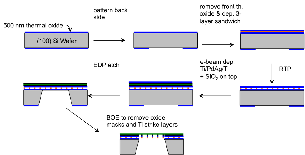
Figure 4: Schematic of concept for creating PdAg film on top of pnc-Si membrane.