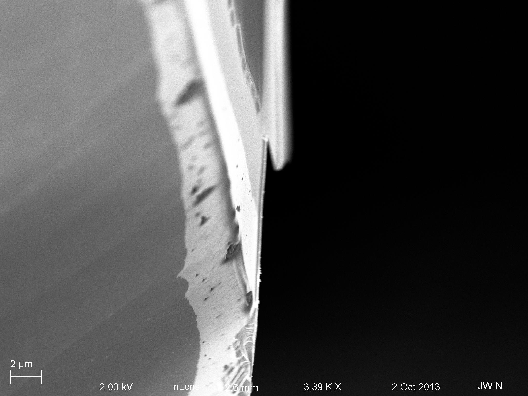
Boron doped c-Si substrate to create silicon lattice under membrane
Hopefully many more details to follow, but JP, Josh M. and I doped some Si substrates with boron using a spin-on-glass. It seems well known that heavily boron doped Si is more resistant to EDP etch than intrinsic or n-type material. We went big and used the 3-slot SEPCON mask.
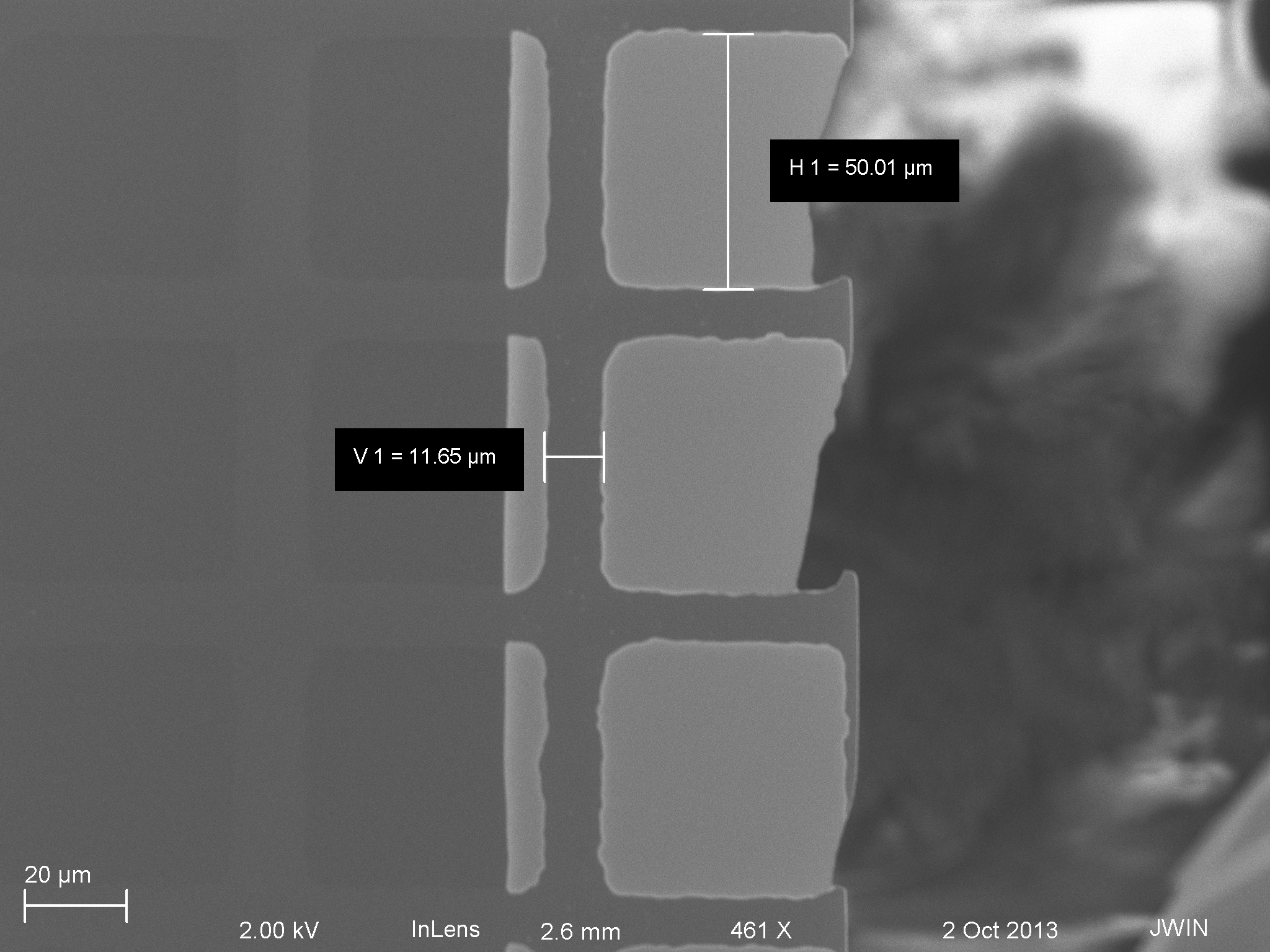

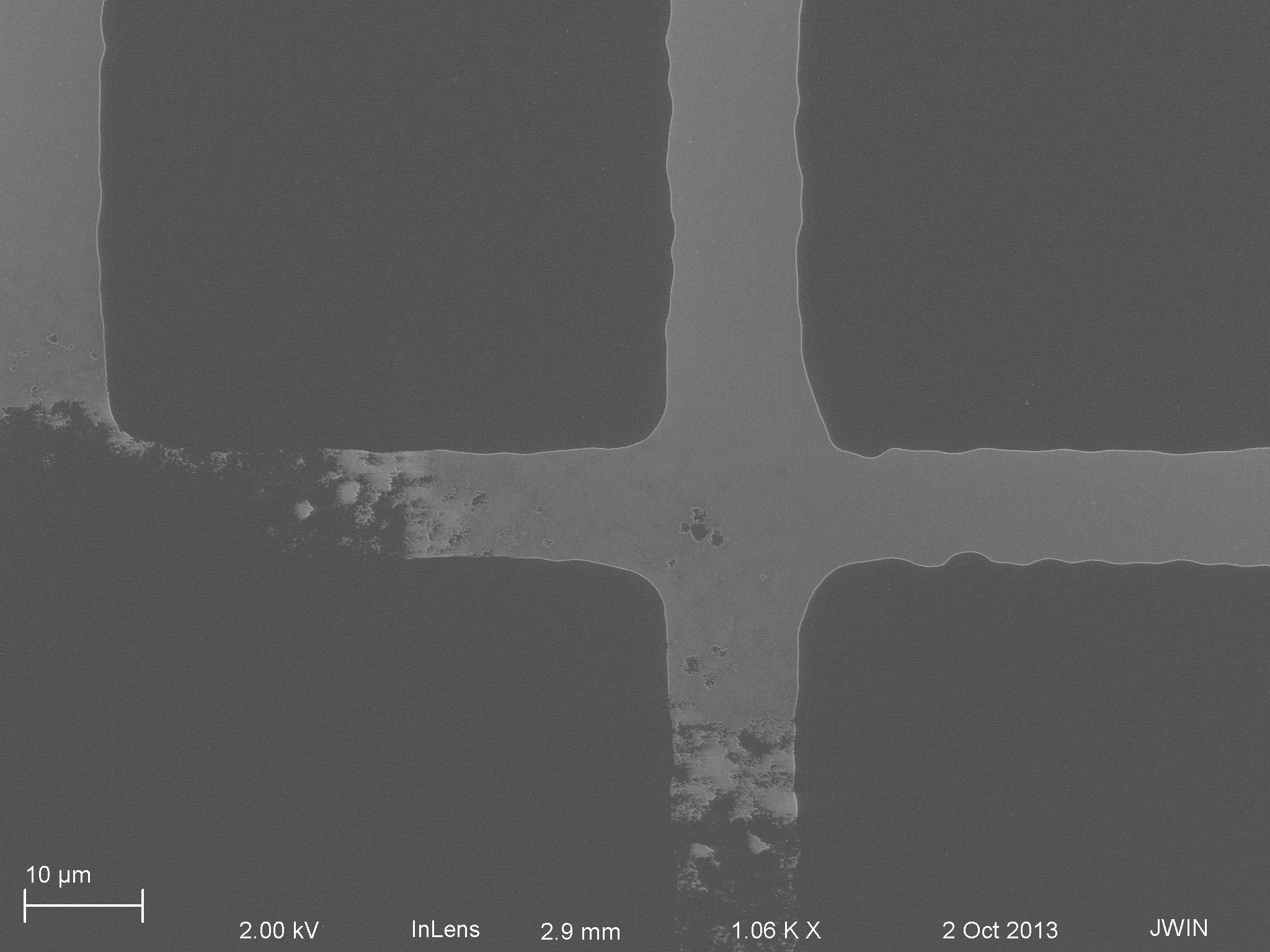
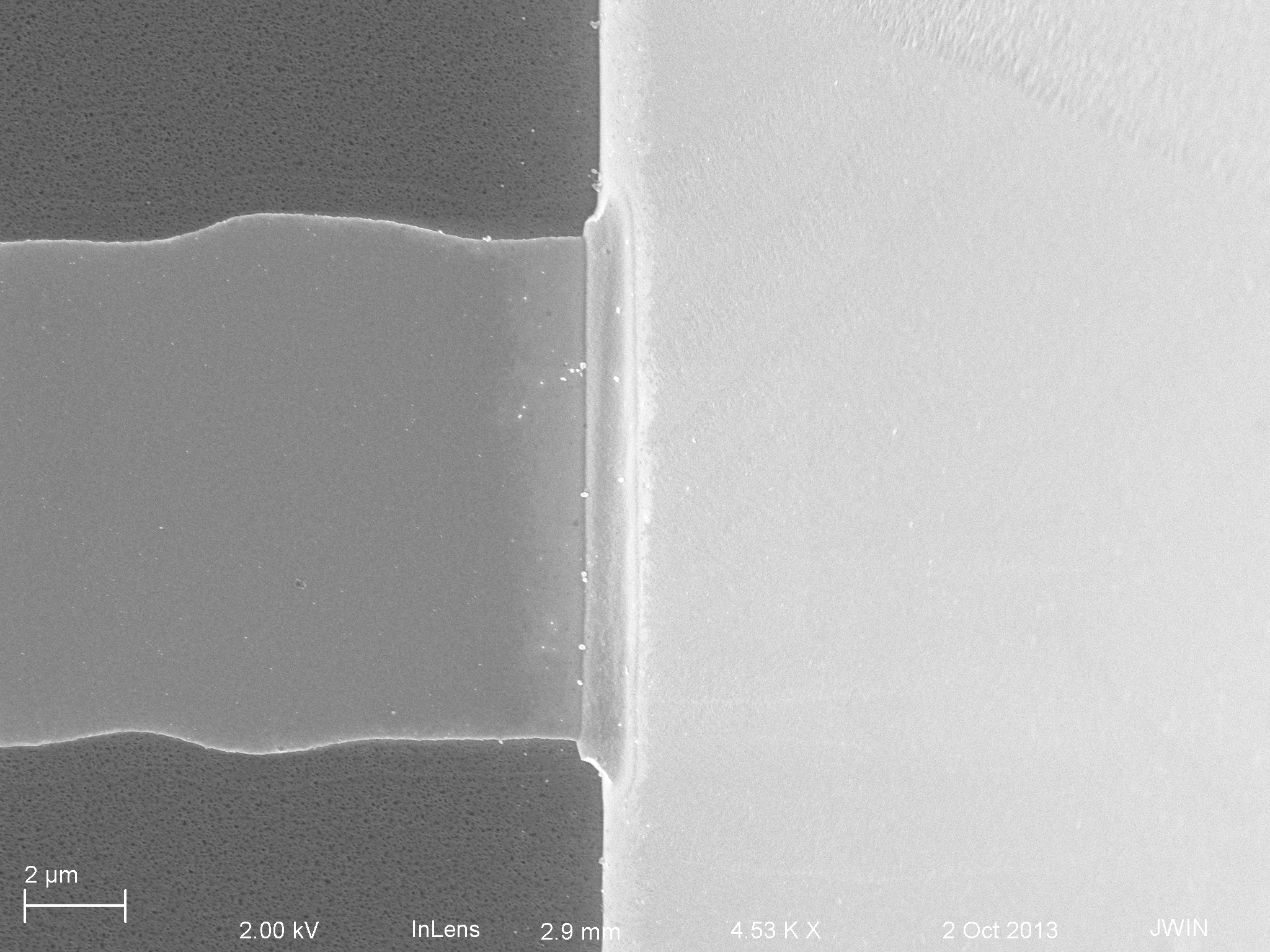
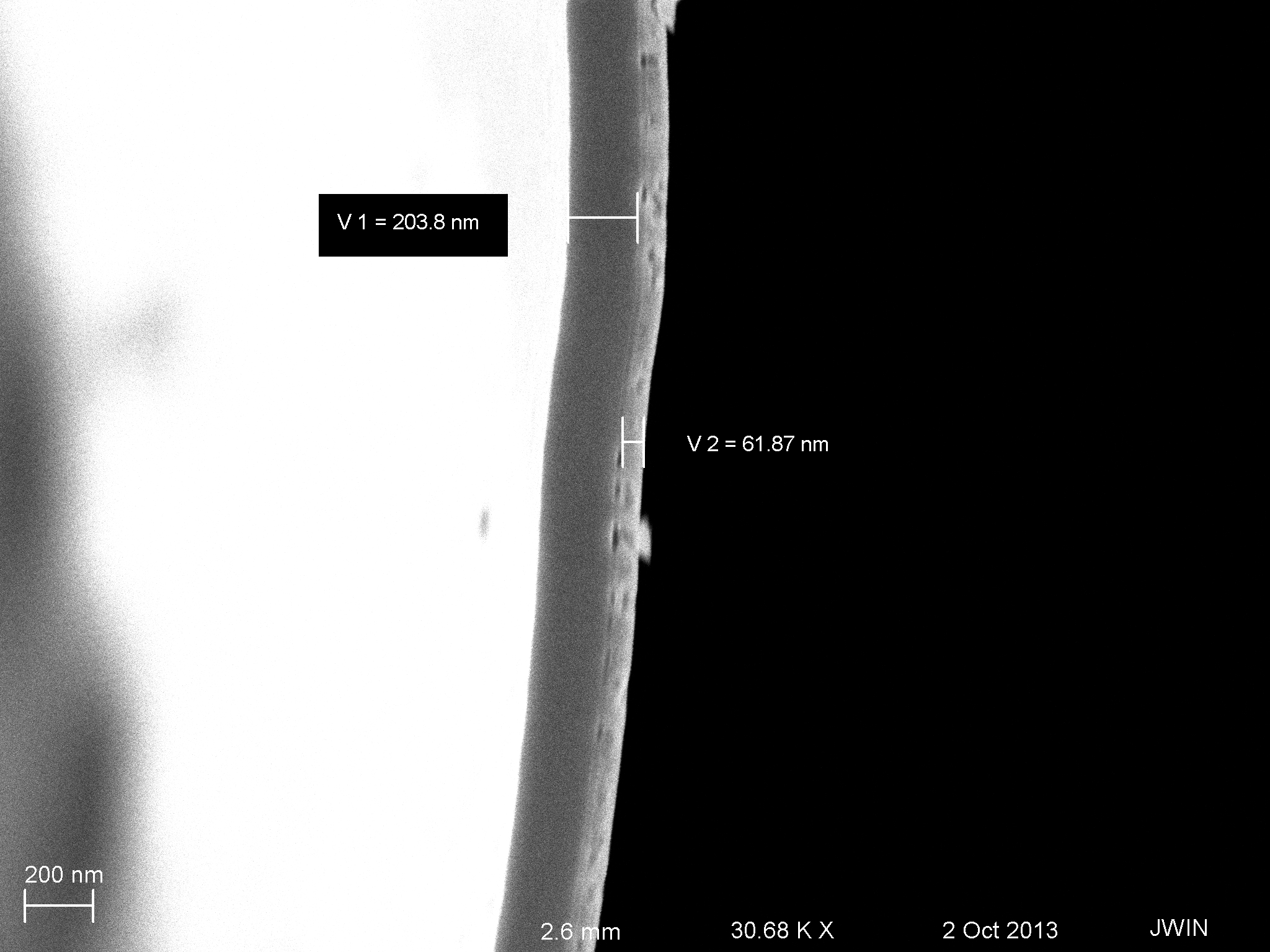
So at least some areas have a 200 nm thick remaining c-Si lattice.
Unfortunately, most of the wafer had no lattice on the chips and we only had about 10% with any lattice. I don’t think any chips had a full lattice remaining under the window.