Anodic Bonding Setup at U of R
Previous Posts Anodic Bonding Theory, Anodic Bonding at RIT
I’ve put together an anodic bonder setup here at the U of R and will be moving it inside the cleanroom shortly.

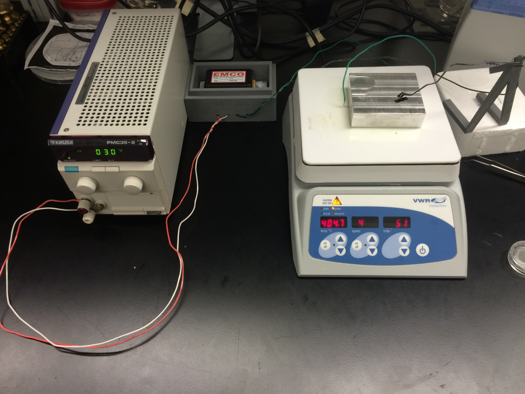
I tried a couple of known combinations to see if the bonder was working properly. The general principle is to liberate sodium ions from glass (move to anode), and allow oxygen to move to the interface (move to cathode), reacting at the interface with the other substrate’s silicon material to make silicon oxide, forming a bond. Ions in the non-glass substrate must be prevented from leaching out into the glass; the high electric field must be maintained at the interface to promote the oxidation.
Si-Coverslip, single interface (400 C, 30 minutes, ~500 V)
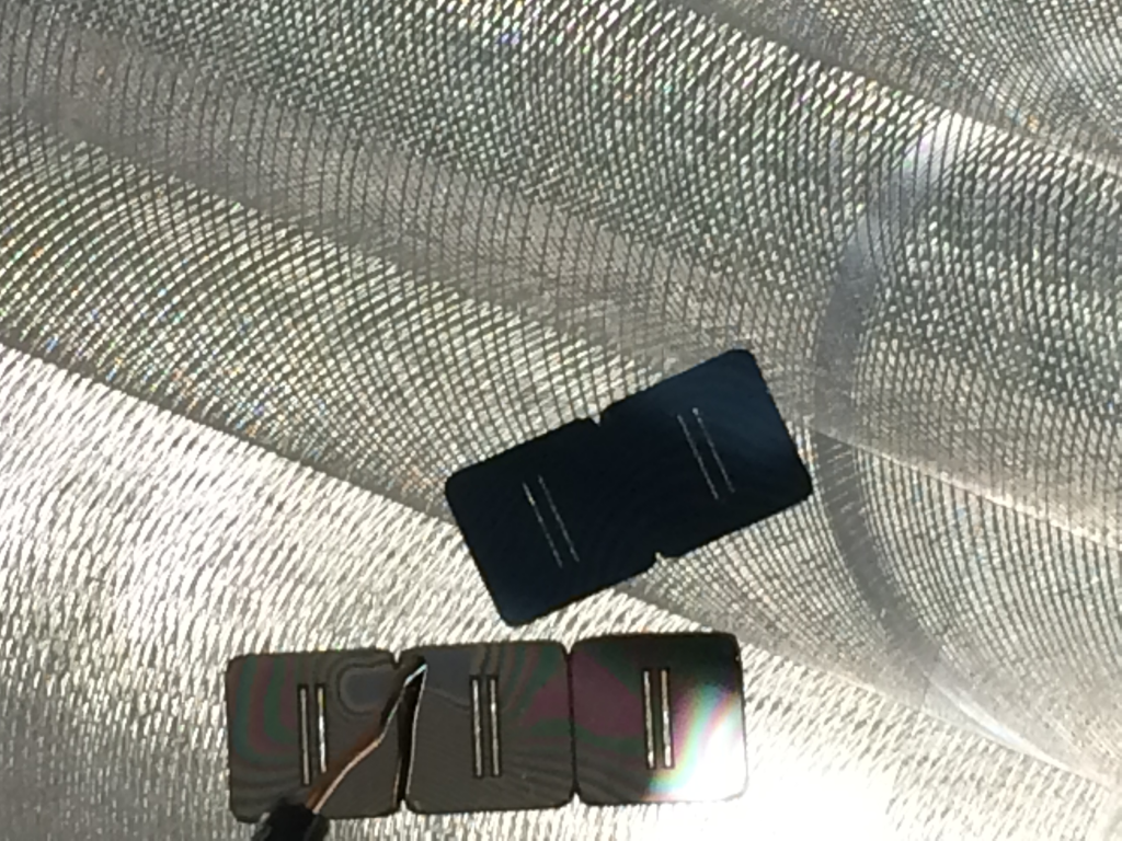
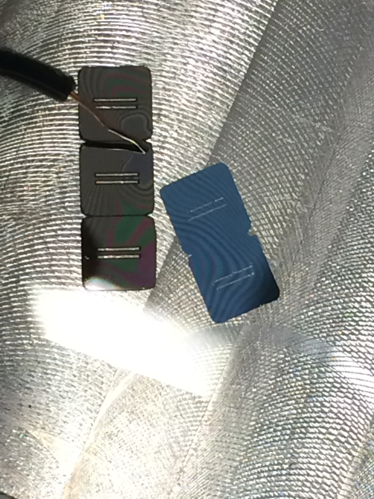

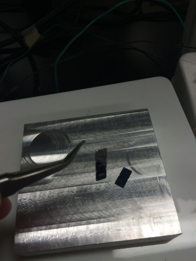
Silicon Nitride – Coverslip (400 C, 30 minutes, ~650V)
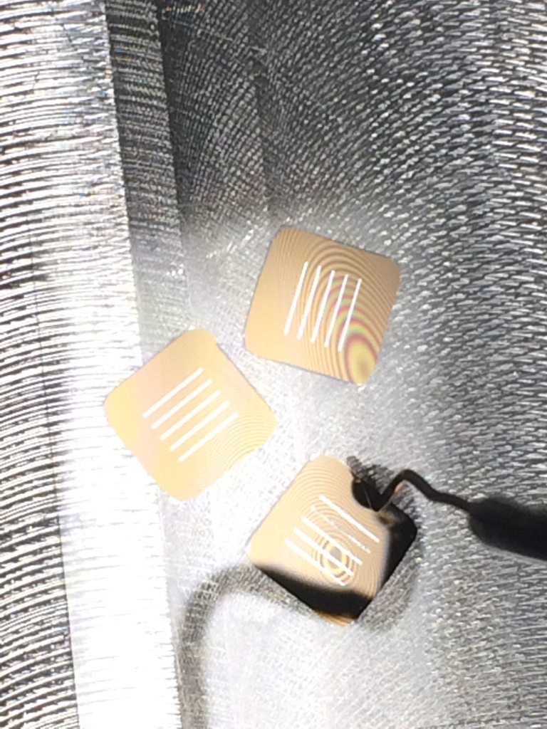

Everything seems to be working appropriately. Now we will have to see if there is enough impurity to make the bond work for the flowchip/oxide channel combination.