MgF2 E-beam Deposition
I am attempting to fabricate a free standing, porous, MgF2 nanomembrane for Raman spectroscopy applications (see my previous post for background). To that end, I’ve used the Lesker p75 evaporator in the basement to deposit ~100nm of MgF2 on one of our nanonitride Sepcon chips (Wafer 1055, 50 nm SiN, 2% porosity, 20-40 nm pores).
I loaded up a crucible 2/3 full with MgF2 pellets, and used a 6 kV source power setting, compared to strict metals at 10 kV. I performed the deposition manually based on Alex Mann’s advice, the chief reason being more control over the deposition rate. I originally wanted to deposit at 0.5 nm/s, however in practice 0.15 nm/s was about all I could achieve. The main source of error here is melting material in a new crucible and attempting to get a steady rate. With manual control, I can steer the beam into new material, which is not possible in an automated recipe, relying on only beam current to modulate the deposition rate. That being said, with a good crucible melt, I should be able to write a recipe for this procedure in the future.
I was apprehensive about depositing thin layers of the material onto the SiN, which I believe will be more stressful and cause the evaporated film to rupture, so I elected to deposit a substantially thicker film for my first run. Once I found a relatively steady position in the crucible, I ramped the beam current from 3-9 mA, keeping the deposition rate hovering in the range between 0.13-0.17 nm/s. The detector registered 1.077 nm when I closed the substrate shutter.
Observations
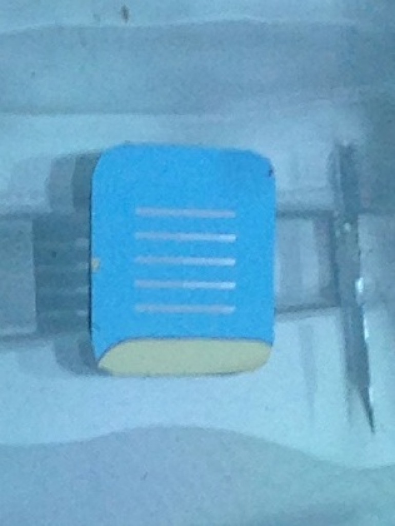
The deposited film turns the SEPCON into a blue chip, from a tan chip at these thicknesses. The film can be scratched with pointed tweezers, but isn’t continuously flaking off from the scratch, suggesting a decent adherence to the lower film. Observation under a phase microscope shows no wrinkling from stress mismatches with the lower film. The membrane isn’t broken anywhere.
Update 12/9/2013
Josh Winans was kind enough to get some crossections of this chip and a few others on the UR SEM. I ran another run of the recipe outlined in this post (reported 104 nm), this time including some pnc-Si TEM grids with the Silicon Nitride scaffold.

Overall, our process control seems to be acceptable for getting a desired film thickness (I’m using +/- 10% as a rule of thumb). The pores are completely occluded in this deposition, expected because of the larger film thickness. Microporous substrates would be perfectly open in this case.
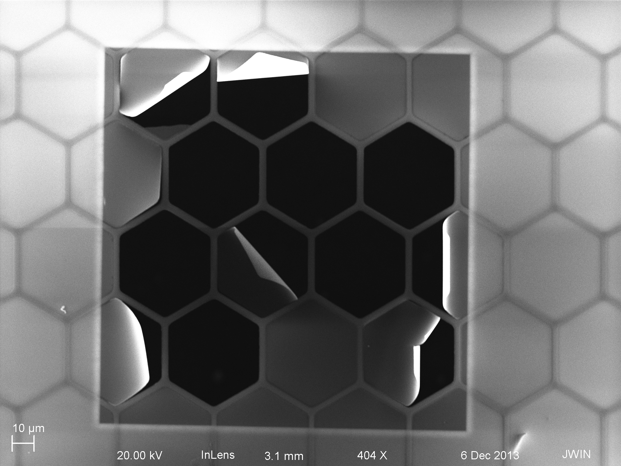
Here is a bulk view of one of the pnc-Si TEM grids with honeycomb support (Single Slot dialysis wafer). The evaporation process has wrenched the pnc-si from the honeycomb support; anybody need some 100 micron hexes of MgF2-pncSi? A really pretty defect.

Closeup view of the defect along the Si3N4 honeycomb. All the literature I’ve read says that multi-layer stacks of MgF2 are very difficult to produce, if not impossible, given high-stress nature of the film.
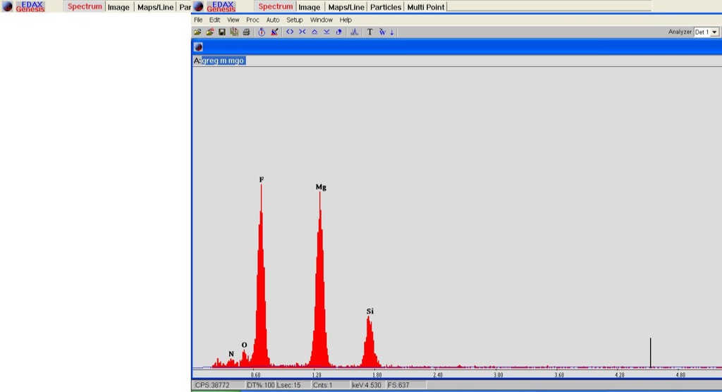
EDS doesn’t show anything troubling in the film that we wouldn’t expect. I performed my evaporation in the microtorr range; really high purity films can occur in the 10 nanotorr range. No contamination from tungsten or gold appears to be present (common materials in our evaporator).
Next Steps
The big test will be to see if we can create a freestanding membrane from the nano nitride structure, without breaking the film. I’m planning to try a hot Phosphoric acid dip to remove the nitride. I will throw in a few SiO2 substrates in the next batch run to see if I can reproduce the unwrinkled membrane with the weaker substrate (removed in BOE) pure SiO2 substrates lacking the honeycomb grid for kicks. It looks like the defects are originating around the honeycomb. Maybe removing nucleation sites for stress propagation will allow the pnc-Si to serve as a scaffold? It’s a fairly long shot though; the film stress is curling the popped silicon hexes pretty heavily.
If the nitride removal is successful (a big if), I will try the same process with a thinner evaporated film. It might be possible that we wouldn’t need to run a physical etch (to transfer the nanopores) at all if the holes in the underlying substrate are large enough to not fuse when the full thickness of the evaporated film is deposited.