Wafer-scale permeance test


(Meghan Kazanski actually did all the work, but she didn’t have a login when this post was started.)
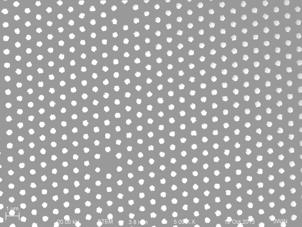
The calculated porosity is 16.4 % with an average pore diameter of 417 nm.
SepCon assembly was performed with chips from wafer 4409. Assembly was performed systematically – SepCons were boxed following assembly for later control testing. General chip locations with respect to the wafer were noted.
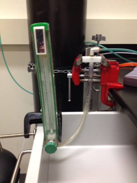
For every ~20 assembled devices, permeance testing was performed to determine flow rate (air at 1 psi). Higher flow rates correspond with higher permeance. Rates were recorded as arbitrary ‘tick’ units (later determined to indicate 1 tick = 0.1 L/min.) Average flow rate was determined as 500±21 ml/min.
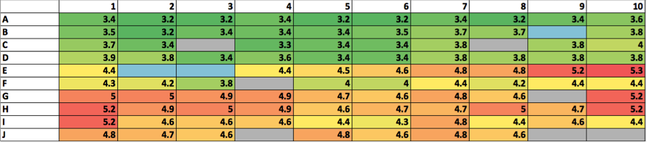
Testing was completed on control SepCons including chips overetched, with lithography imperfections, ruptured membranes, and the exclusion of either the ‘U’ or ‘square’ gasket (see Box I testing data below).
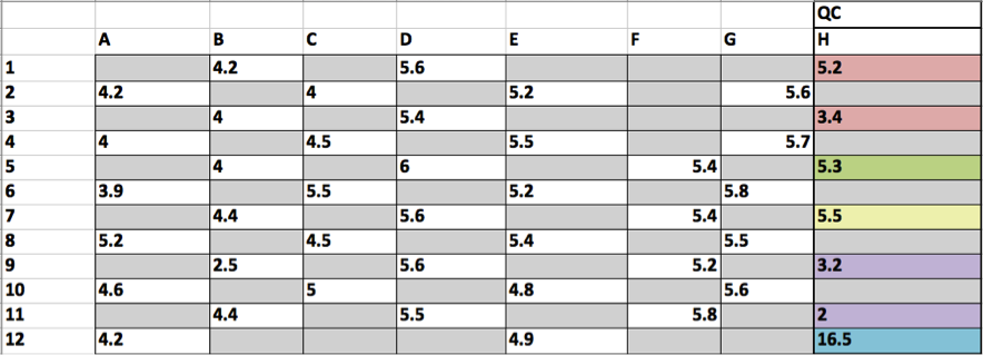
Blue = ruptured
Green = no ‘U’ gasket
Yellow = No ‘square’ gasket
Purple = Litho imperfections
As assembly and testing progressed, a suspected trend developed between chip wafer location of and flow rate , potentially due to imperfect uniformity in fabrication process affecting pore size/ presence. The most likely cause of this non-uniformity is the RIE etch process.
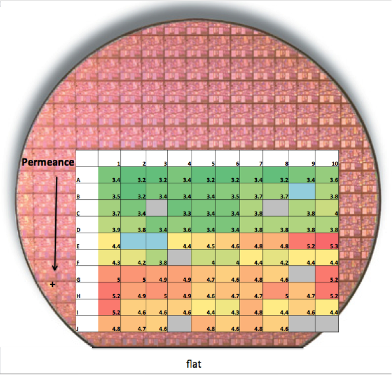
Radial testing was performed on series of chips (see wafer map and heat map below). This confirmed that flow rates did increase with radial distance from wafer center, according to produced heat map. The table is overlaid on a stock silicon wafer photo for context.