Gate-Voltage-Dependent EO Pumping: -6 V on the Gate Changes the Pumping Rate by an Order of Magnitude
In my previous post on applying voltage to a silver-coated NPN chip, I put up a video which, if you squinted and were willing to be charitable, showed that I could modify the EO pumping behavior of the chip by applying 2 V to the membrane. I repeated the experiment, and I think I can say much more firmly that a silver-coated NPN chip can act as a nanofluidic transistor. In fact, we can say that a -6 V gate voltage results in an order of magnitude change in pumping rate!
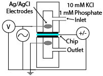
Video of Pumping (shared via google drive). In this video, I apply a square wave of +/- 10 V at a frequency of 0.2 Hz (a flip every 5 seconds, although in the video it looks closer to 3 second flips) to two electrodes across the membrane.
The markings showed in the video are from a microscope calibration slide and are 100 um. Since the tubing is 1/32” ID, it has a volume of 0.05024 mm^3 (or 0.05024 uL) per tick mark. As long as no voltage is applied to the membrane, pumping is minimal (about a half tick per flip, or 0.025 uL / 3s, or ~ 8 nL/s). When -6 V is applied to the gate, the pumping rate is significant (although, weirdly, only in one direction, which I think is due to a slight pressure gradient in the system arising from the arraignment of the tubes) higher, at ~ 3 ticks per flip, or ~50nL/s. When +6V is applied to the gate, you might be able to convince yourself that the pumping rate is even lower than when no voltage is applied, but you’d need to really stare at that video. Note that in calculating these rates, I have ignored the ‘meniscus inverting’ effects.
I’m not particularly happy with using the microscope calibration slide as measure of volume passed, and because making and inserting the chips requires a considerable amount of time, I’m refraining from doing any more EO work until I have a better way of getting rates. That said, the EO I get with untreated pnc-Si with +/- 10 V square wave is comparable to that of the -6 V applied to the gate case.
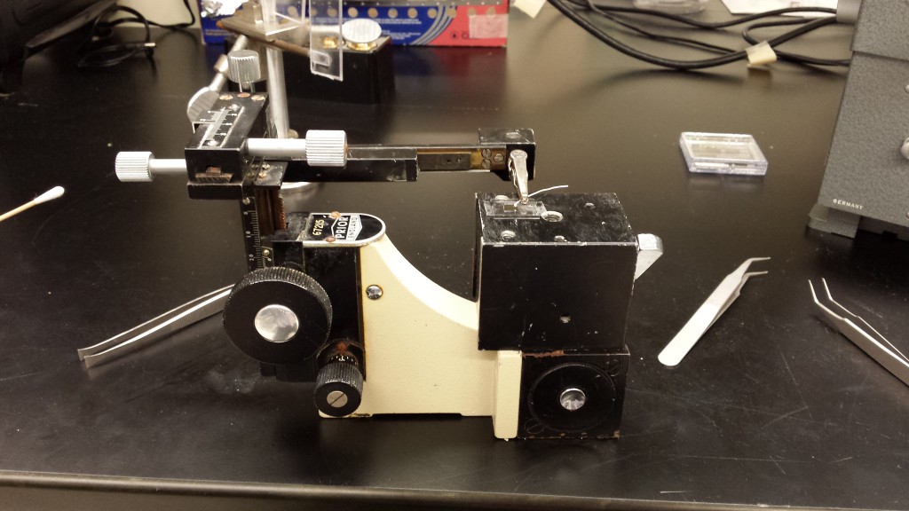
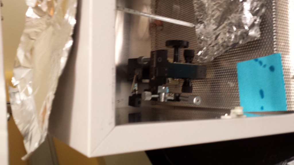
One of the problems I’ve had with collecting this data is that it is very difficult to place a lead onto the corner of the chip so that there is enough room for the circular gasket to seal the chip, as shown in this picture from my last NFT efforts:


I’ve broken a few chips after trying to put them in, and so I dug around in the lab and found a pair of micromanipulators to help me make and insert the chips:
In this picture, the micromanipulator holds a piece of Ag/AgCl ink-coated silver wire.
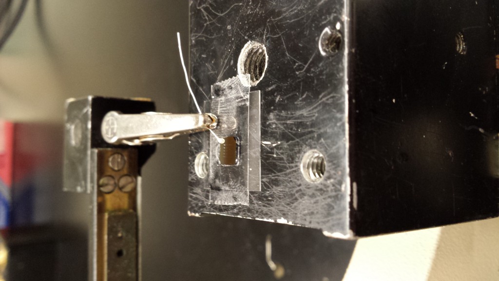
When the wire is affixed, the entire assembly is placed in the oven.
A second micromanipulator is used for inserting the chips into the gap between the acrylic rods in the zetapotential/EO setup.
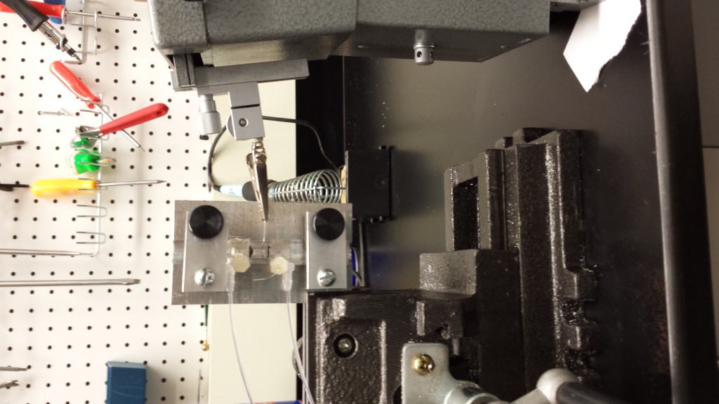
The weight of the wire and the need for placing the chip perfectly necessitates the micromanipulator, although thankfully when chips without leads are inserted all that’s needed is a steady hand.
For what it’s worth, I made 20 of these silver NFT’s. I broke 2 during depositions (my glove caught the windows while I was removing the kapton tape that affixed them to the PVD-75b platen), 1 during the wire-bonding stage (I hadn’t figured out the vagaries of my micromanipulator setup yet) and it took me three chips to get one into the acrylic gap (mostly because I had placed the wires too close to the membrane windows). It takes me ~1 hour on the PVD (at $24/hr) and 0.5 hour on the ALD (at $24/hr) to make them. The biggest rate-limiting steps are affixing/removing the chips with kapton in the PVD, and using silver epoxy to attach the wire leads.
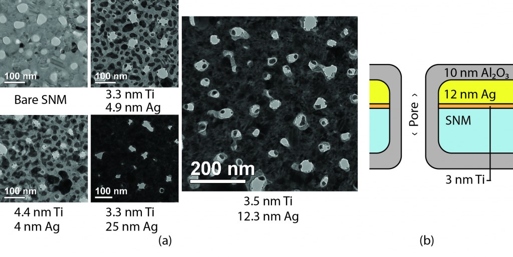
For reference, here is the stack on the chip: